SBOS350B December 2006 – December 2024 OPA4830
PRODUCTION DATA
- 1
- 1 Features
- 2 Applications
- 3 Description
- 4 Related Products
- 5 Pin Configuration and Functions
-
6 Specifications
- 6.1 Absolute Maximum Ratings
- 6.2 ESD Ratings
- 6.3 Recommended Operating Conditions
- 6.4 Thermal Information
- 6.5 Electrical Characteristics VS = ±5V
- 6.6 Electrical Characteristics VS = 5V
- 6.7 Electrical Characteristics VS = 3V
- 6.8 Typical Characteristics: VS = ±5V
- 6.9 Typical Characteristics: VS = ±5V, Differential Configuration
- 6.10 Typical Characteristics: VS = 5V
- 6.11 Typical Characteristics: VS = 5V, Differential Configuration
- 6.12 Typical Characteristics: VS = 3V
- 6.13 Typical Characteristics: VS = 3V, Differential Configuration
- 7 Parameter Measurement Information
-
8 Application and Implementation
- 8.1
Application Information
- 8.1.1 Wideband Voltage-Feedback Operation
- 8.1.2 DC Level-Shifting
- 8.1.3 AC-Coupled Output Video Line Driver
- 8.1.4 Noninverting Amplifier With Reduced Peaking
- 8.1.5 Single-Supply Active Filter
- 8.1.6 Differential Interface Applications
- 8.1.7 DC-Coupled Single-to-Differential Conversion
- 8.1.8 Low-Power, Differential I/O, 4th-Order Active Filter
- 8.1.9 Dual-Channel, Differential ADC Driver
- 8.1.10 Video Line Driving
- 8.1.11 4-Channel DAC Transimpedance Amplifier
- 8.1.12 Operating Suggestions: Optimizing Resistor Values
- 8.1.13 Bandwidth vs Gain: Noninverting Operation
- 8.1.14 Inverting Amplifier Operation
- 8.1.15 Output Current and Voltages
- 8.1.16 Driving Capacitive Loads
- 8.1.17 Distortion Performance
- 8.1.18 Noise Performance
- 8.1.19 DC Accuracy and Offset Control
- 8.2 Power Supply Recommendations
- 8.3 Layout
- 8.1
Application Information
- 9 Device and Documentation Support
- 10Revision History
- 11Mechanical, Packaging, and Orderable Information
Package Options
Refer to the PDF data sheet for device specific package drawings
Mechanical Data (Package|Pins)
- PW|14
Thermal pad, mechanical data (Package|Pins)
Orderable Information
8.1.6 Differential Interface Applications
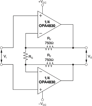
Dual and quad op amps are particularly designed to differential input to differential output applications. Typically, these op amps fall into either ADC input interface or line driver applications. Two basic approaches to differential I/O are noninverting or inverting configurations. Because the output is differential, the signal polarity is somewhat meaningless—the noninverting and inverting terminology applies here to where the input is brought into the OPA4830. Each has advantages and disadvantages. Figure 8-9 shows a basic starting point for noninverting differential I/O applications.
This approach provides for a source termination impedance that is independent of the signal gain. For instance, simple differential filters can be included in the signal path right up to the noninverting inputs without interacting with the amplifier gain. The differential signal gain for the circuit of Figure 8-9 is shown in Equation 6:

Figure 8-9 shows the recommended value of 750Ω. However, the gain can be adjusted using just the RG resistor.
 Figure 8-9 Noninverting Differential I/O
Amplifier
Figure 8-9 Noninverting Differential I/O
AmplifierVarious combinations of single-supply or ac-coupled gains can also be delivered using the basic circuit of Figure 8-9. Common-mode bias voltages on the two noninverting inputs pass on to the output with a gain of 1V/V because an equal dc voltage at each inverting node creates no current through RG, giving that voltage a common-mode gain of 1 to the output.
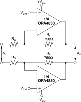
Figure 8-10 shows a differential I/O stage configured as an inverting amplifier. In this case, the gain resistors (RG) become the input resistance for the source. This configuration provides a better noise performance than the noninverting configuration, but does limit the flexibility in setting the input impedance separately from the gain.
 Figure 8-10 Inverting Differential I/O
Amplifier
Figure 8-10 Inverting Differential I/O
AmplifierThe two noninverting inputs provide an easy common-mode control input. This control is particularly useful if the source is ac-coupled through either blocking caps or a transformer. In either case, the common-mode input voltages on the two noninverting inputs again have a gain of 1 to the output pins, giving an easy common-mode control for single-supply operation. The input resistors can be adjusted to the desired gain but also change the input impedance as well. The differential gain for this circuit is shown in Equation 7:
