SLVSET9F September   2018  – February 2023 TPS1663

PRODUCTION DATA  

  1. Features
  2. Applications
  3. Description
  4. Revision History
  5. Device Comparison Table
  6. Pin Configuration and Functions
  7. Specifications
    1. 7.1 Absolute Maximum Ratings
    2. 7.2 ESD Ratings
    3. 7.3 Recommended Operating Conditions
    4. 7.4 Thermal Information
    5. 7.5 Electrical Characteristics
    6. 7.6 Timing Requirements
    7. 7.7 Typical Characteristics
  8. Parameter Measurement Information
  9. Detailed Description
    1. 9.1 Overview
    2. 9.2 Functional Block Diagram
    3. 9.3 Feature Description
      1. 9.3.1  Hot Plug-In and In-Rush Current Control
        1. 9.3.1.1 Thermal Regulation Loop
      2. 9.3.2  Undervoltage Lockout (UVLO)
      3. 9.3.3  Overvoltage Protection (OVP)
      4. 9.3.4  Overload and Short Circuit Protection
        1. 9.3.4.1 Overload Protection
        2. 9.3.4.2 Short Circuit Protection
          1. 9.3.4.2.1 Start-Up With Short-Circuit On Output
      5. 9.3.5  Output Power Limiting, PLIM (TPS16632 Only)
      6. 9.3.6  Current Monitoring Output (IMON)
      7. 9.3.7  FAULT Response (FLT)
      8. 9.3.8  Power Good Output (PGOOD)
      9. 9.3.9  IN, P_IN, OUT and GND Pins
      10. 9.3.10 Thermal Shutdown
      11. 9.3.11 Low Current Shutdown Control (SHDN)
    4. 9.4 Device Functional Modes
  10. 10Application and Implementation
    1. 10.1 Application Information
    2. 10.2 Typical Application
      1. 10.2.1 Design Requirements
      2. 10.2.2 Detailed Design Procedure
        1. 10.2.2.1 Programming the Current-Limit Threshold R(ILIM) Selection
        2. 10.2.2.2 Undervoltage Lockout and Overvoltage Set Point
        3. 10.2.2.3 Setting Output Voltage Ramp Time (tdVdT)
          1. 10.2.2.3.1 Support Component Selections RPGOOD and C(IN)
      3. 10.2.3 Application Curves
    3. 10.3 System Examples
      1. 10.3.1 Simple 24-V Power Supply Path Protection
    4. 10.4 Power Supply Recommendations
      1. 10.4.1 Transient Protection
    5. 10.5 Layout
      1. 10.5.1 Layout Guidelines
      2. 10.5.2 Layout Example
  11. 11Device and Documentation Support
    1. 11.1 Documentation Support
      1. 11.1.1 Related Documentation
    2. 11.2 Receiving Notification of Documentation Updates
    3. 11.3 Support Resources
    4. 11.4 Trademarks
    5. 11.5 Electrostatic Discharge Caution
    6. 11.6 Glossary
  12. 12Mechanical, Packaging, and Orderable Information

Package Options

Refer to the PDF data sheet for device specific package drawings

Mechanical Data (Package|Pins)
  • RGE|24
  • PWP|20
Thermal pad, mechanical data (Package|Pins)
Orderable Information

Typical Characteristics

–40°C ≤ TA = TJ ≤ +125°C, V(IN) = V(P_IN) = 24 V, V( SHDN) = 2 V, R(ILIM) = 30 kΩ, IMON = PGOOD = FLT = OPEN, C(OUT) = 1 μF, C(dVdT) = OPEN (unless stated otherwise)
GUID-775925CB-1C8E-4461-90A3-E7DA6BA1DC37-low.gif
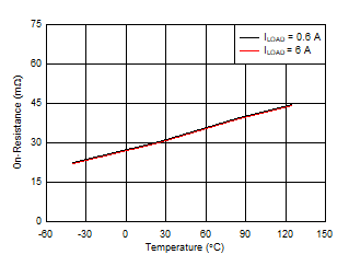
Figure 7-1 On-Resistance vs Temperature Across Load Current
GUID-13F3C08C-6DFF-4A4F-A4AB-3CC1DA7E3FD6-low.gif
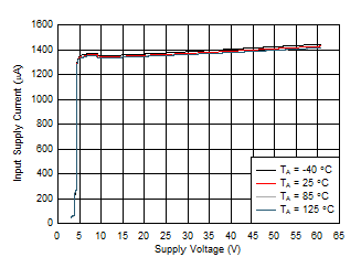
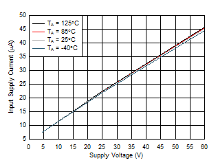
Figure 7-3 Input Supply Current vs Supply Voltage in Shutdown
GUID-94430FD1-C0B3-4D3A-9BB8-1399FC290683-low.gif
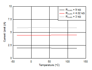
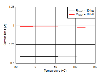
Figure 7-5 Overload Current Limit vs Temperature
GUID-C6050CDC-53F2-46D5-9341-B988474228BC-low.gif
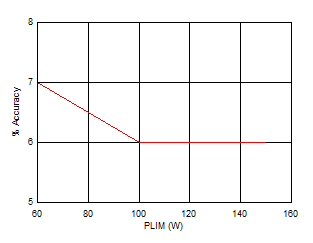
Figure 7-7 Output Power Limiting Accuracy vs PLIM
GUID-9DBC581E-CCE8-4F2F-99DB-132EB32903CF-low.gif
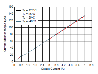
Figure 7-9 Current Monitor Output vs Output Current
GUID-1E4BFAC6-6F17-41E9-83A7-081AA170C779-low.gif
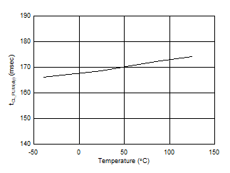
Figure 7-11 Maximum Duration in Current and Power Limiting vs Temperature
GUID-4C9004D9-65BE-4AC1-8EEC-727DF6D2E32F-low.gif
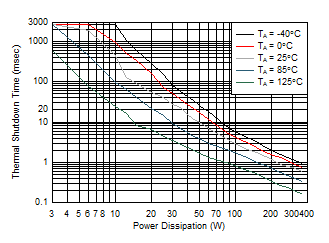
Taken on VQFN device on EVM Board
Figure 7-13 Thermal Shutdown Time vs Power Dissipation
GUID-666B42A6-153B-4CEF-AD1F-D4C237930785-low.gif
TPS16632
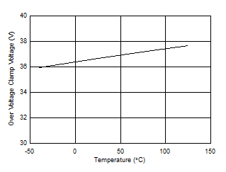
Figure 7-2 Overvoltage Clamp Threshold vs Temperature
GUID-2E0EEA0F-1AE2-4DFC-BDFE-A76DABC87AE3-low.gif
Figure 7-4 Input Supply Current vs Supply Voltage During Normal Operation
GUID-58A3A813-A3BE-46F2-900E-0C0C36F5E141-low.gif
Figure 7-6 Overload Current Limit vs Temperature
GUID-922736B2-0341-4A91-8E64-EA2ED12B4ED0-low.gif
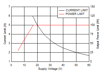
TPS16632 R(PLIM) = 100 kΩ R(ILIM) = 3 kΩ
Figure 7-8 Power Limit, Current Limit vs Supply Voltage
GUID-BE31A47D-04D9-49FB-9699-40BB8E284ACC-low.gif
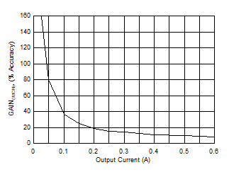
Figure 7-10 IMON Gain Accuracy at Low Output Current Levels
GUID-3F399230-8674-46FF-8B5A-E345D5C863D7-low.gif
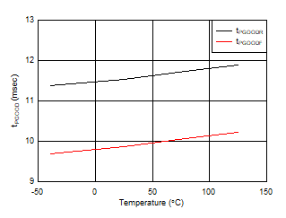
Figure 7-12 PGOOD Rising and Falling Delay vs Temperature