SLVSET9F September 2018 – February 2023 TPS1663
PRODUCTION DATA
- 1 Features
- 2 Applications
- 3 Description
- 4 Revision History
- 5 Device Comparison Table
- 6 Pin Configuration and Functions
- 7 Specifications
- 8 Parameter Measurement Information
-
9 Detailed Description
- 9.1 Overview
- 9.2 Functional Block Diagram
- 9.3
Feature Description
- 9.3.1 Hot Plug-In and In-Rush Current Control
- 9.3.2 Undervoltage Lockout (UVLO)
- 9.3.3 Overvoltage Protection (OVP)
- 9.3.4 Overload and Short Circuit Protection
- 9.3.5 Output Power Limiting, PLIM (TPS16632 Only)
- 9.3.6 Current Monitoring Output (IMON)
- 9.3.7 FAULT Response (FLT)
- 9.3.8 Power Good Output (PGOOD)
- 9.3.9 IN, P_IN, OUT and GND Pins
- 9.3.10 Thermal Shutdown
- 9.3.11 Low Current Shutdown Control (SHDN)
- 9.4 Device Functional Modes
- 10Application and Implementation
- 11Device and Documentation Support
- 12Mechanical, Packaging, and Orderable Information
Package Options
Refer to the PDF data sheet for device specific package drawings
Mechanical Data (Package|Pins)
- RGE|24
- PWP|20
Thermal pad, mechanical data (Package|Pins)
Orderable Information
9.3.1 Hot Plug-In and In-Rush Current Control
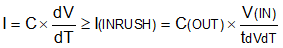
The devices are designed to control the in-rush current upon insertion of a card into a live backplane or other hot power source. This design limits the voltage sag on the backplane’s supply voltage and prevents unintended resets of the system power. The controlled start-up also helps to eliminate conductive and radiative interferences. An external capacitor connected from the dVdT pin to GND defines the slew rate of the output voltage at power-on. The fastest output slew rate of 24 V/500 µs can be achieved by leaving dVdT pin floating. The inrush current can be calculated using #T5006940-1IN.
where
#INRUSH_DVDT illustrates in-rush current control performance of the device during Hot Plug-In.

| CdVdT = 100 nF | COUT = 1000 µF | RILIM = 4.02 kΩ |