SNVSBF6B October 2019 – December 2020 TPSM265R1
PRODUCTION DATA
- 1 Features
- 2 Applications
- 3 Description
- 4 Revision History
- 5 Pin Configuration and Functions
-
6 Specifications
- 6.1 Absolute Maximum Ratings
- 6.2 ESD Ratings
- 6.3 Recommended Operating Conditions
- 6.4 Thermal Information
- 6.5 Electrical Characteristics
- 6.6 Typical Characteristics (VIN = 5 V)
- 6.7 Typical Characteristics (VIN = 12 V)
- 6.8 Typical Characteristics (VIN = 24 V)
- 6.9 Typical Characteristics (VIN = 48 V)
- 6.10 Typical Characteristics (VIN = 65 V)
-
7 Detailed Description
- 7.1 Overview
- 7.2 Functional Block Diagram
- 7.3
Feature Description
- 7.3.1 Adjustable Output Voltage (FB)
- 7.3.2 Input Capacitor Selection
- 7.3.3 Output Capacitor Selection
- 7.3.4 Precision Enable (EN), Undervoltage Lockout (UVLO), and Hysteresis (HYS)
- 7.3.5 PFM Operation
- 7.3.6 Power Good (PGOOD)
- 7.3.7 Configurable Soft Start (SS)
- 7.3.8 Overcurrent Protection (OCP)
- 7.3.9 Thermal Shutdown
- 7.4 Device Functional Modes
- 8 Applications and Implementation
- 9 Power Supply Recommendations
- 10Layout
- 11Device and Documentation Support
- 12Mechanical, Packaging, and Orderable Information
Package Options
Mechanical Data (Package|Pins)
- SIL|10
Thermal pad, mechanical data (Package|Pins)
Orderable Information
7.3.5 PFM Operation
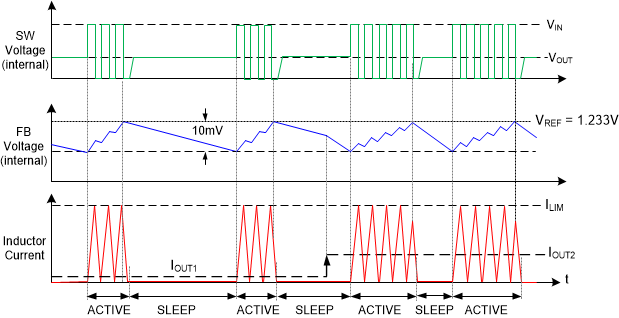
The TPSM265R1 operates in Pulse Frequency Modulation (PFM) mode. The TPSM265R1 behaves as a hysteretic voltage regulator operating within upper and lower feedback regulation thresholds with typical 10 mV of hysteresis. Figure 7-4 is a representation of the relevant voltage waveforms and inductor current waveform. The TPSM265R1 provides the required switching pulses to recharge the output capacitance, followed by a sleep period where most of the internal circuits are shut off. The load current is supported by the output capacitor during this time, and the TPSM265R1 current consumption approaches the sleep quiescent current of 10.5 μA (typ). The sleep period duration depends on load current and output capacitance.
 Figure 7-4 PFM Mode SW Node Voltage, Feedback Voltage, and Inductor Current Waveforms