SNVSBF6B October 2019 – December 2020 TPSM265R1
PRODUCTION DATA
- 1 Features
- 2 Applications
- 3 Description
- 4 Revision History
- 5 Pin Configuration and Functions
-
6 Specifications
- 6.1 Absolute Maximum Ratings
- 6.2 ESD Ratings
- 6.3 Recommended Operating Conditions
- 6.4 Thermal Information
- 6.5 Electrical Characteristics
- 6.6 Typical Characteristics (VIN = 5 V)
- 6.7 Typical Characteristics (VIN = 12 V)
- 6.8 Typical Characteristics (VIN = 24 V)
- 6.9 Typical Characteristics (VIN = 48 V)
- 6.10 Typical Characteristics (VIN = 65 V)
-
7 Detailed Description
- 7.1 Overview
- 7.2 Functional Block Diagram
- 7.3
Feature Description
- 7.3.1 Adjustable Output Voltage (FB)
- 7.3.2 Input Capacitor Selection
- 7.3.3 Output Capacitor Selection
- 7.3.4 Precision Enable (EN), Undervoltage Lockout (UVLO), and Hysteresis (HYS)
- 7.3.5 PFM Operation
- 7.3.6 Power Good (PGOOD)
- 7.3.7 Configurable Soft Start (SS)
- 7.3.8 Overcurrent Protection (OCP)
- 7.3.9 Thermal Shutdown
- 7.4 Device Functional Modes
- 8 Applications and Implementation
- 9 Power Supply Recommendations
- 10Layout
- 11Device and Documentation Support
- 12Mechanical, Packaging, and Orderable Information
Package Options
Mechanical Data (Package|Pins)
- SIL|10
Thermal pad, mechanical data (Package|Pins)
Orderable Information
8.2.2.2 Output Voltage Setpoint
The output voltage of the TPSM265R1 device is externally adjustable using a resistor divider. The recommended value of RFBT is 100 kΩ. The value for RFBB can be selected from Table 7-1 or calculated using Equation 5:
Equation 5. 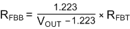
For the desired output voltage of 5 V, the formula yields a value of 32.38 kΩ. Choose the closest available standard value of 32.4 kΩ for RFBB.