SLUSD12A October   2017  – February 2018 UCC28780

PRODUCTION DATA.  

  1. Features
  2. Applications
  3. Description
    1.     Device Images
      1.      Simplified Schematic
      2.      45-W, 20-V GaN-ACF Adapter Efficiency
  4. Revision History
  5. Pin Configuration and Functions
    1.     Pin Functions
  6. Specifications
    1. 6.1 Absolute Maximum Ratings
    2. 6.2 ESD Ratings
    3. 6.3 Recommended Operating Conditions
    4. 6.4 Thermal Information of SOIC
    5. 6.5 Thermal Information of WQFN
    6. 6.6 Electrical Characteristics
    7. 6.7 Typical Characteristics
  7. Detailed Description
    1. 7.1 Overview
    2. 7.2 Functional Block Diagram
    3. 7.3 Detailed Pin Description
      1. 7.3.1 BUR Pin (Programmable Burst Mode)
      2. 7.3.2 FB Pin (Feedback Pin)
      3. 7.3.3 VDD Pin (Device Bias Supply)
      4. 7.3.4 REF Pin (Internal 5-V Bias)
      5. 7.3.5 HVG and SWS Pins
      6. 7.3.6 RTZ Pin (Sets Delay for Transition Time to Zero)
      7. 7.3.7 RDM Pin (Sets Synthesized Demagnetization Time for ZVS Tuning)
      8. 7.3.8 RUN Pin (Driver Enable Pin)
      9. 7.3.9 SET Pin
    4. 7.4 Device Functional Modes
      1. 7.4.1  Adaptive ZVS Control with Auto-Tuning
      2. 7.4.2  Dead-Time Optimization
      3. 7.4.3  Control Law across Entire Load Range
      4. 7.4.4  Adaptive Amplitude Modulation (AAM)
      5. 7.4.5  Adaptive Burst Mode (ABM)
      6. 7.4.6  Low Power Mode (LPM)
      7. 7.4.7  Standby Power Mode (SBP)
      8. 7.4.8  Startup Sequence
      9. 7.4.9  Survival Mode of VDD
      10. 7.4.10 System Fault Protections
        1. 7.4.10.1 Brown-In and Brown-Out
        2. 7.4.10.2 Output Over-Voltage Protection
        3. 7.4.10.3 Over-Temperature Protection
        4. 7.4.10.4 Programmable Over-Power Protection
        5. 7.4.10.5 Peak Current Limit
        6. 7.4.10.6 Output Short-Circuit Protection
        7. 7.4.10.7 Over-Current Protection
        8. 7.4.10.8 Thermal Shutdown
      11. 7.4.11 Pin Open/Short Protections
        1. 7.4.11.1 Protections on CS pin Fault
        2. 7.4.11.2 Protections on HVG pin Fault
        3. 7.4.11.3 Protections on RDM and RTZ pin Faults
  8. Application and Implementation
    1. 8.1 Application Information
    2. 8.2 Typical Application Circuit
      1. 8.2.1 Design Requirements
      2. 8.2.2 Detailed Design Procedure
        1. 8.2.2.1 Input Bulk Capacitance and Minimum Bulk Voltage
        2. 8.2.2.2 Transformer Calculations
          1. 8.2.2.2.1 Primary-to-Secondary Turns Ratio (NPS)
          2. 8.2.2.2.2 Primary Magnetizing Inductance (LM)
          3. 8.2.2.2.3 Primary Turns (NP)
          4. 8.2.2.2.4 Secondary Turns (NS)
          5. 8.2.2.2.5 Turns of Auxiliary Winding (NA)
          6. 8.2.2.2.6 Winding and Magnetic Core Materials
        3. 8.2.2.3 Clamp Capacitor Calculation
        4. 8.2.2.4 Bleed-Resistor Calculation
        5. 8.2.2.5 Output Filter Calculation
        6. 8.2.2.6 Calculation of ZVS Sensing Network
        7. 8.2.2.7 Calculation of Compensation Network
      3. 8.2.3 Application Curves
  9. Power Supply Recommendations
  10. 10Layout
    1. 10.1 Layout Guidelines
      1. 10.1.1 General Considerations
      2. 10.1.2 RDM and RTZ Pins
      3. 10.1.3 SWS Pin
      4. 10.1.4 VS Pin
      5. 10.1.5 BUR Pin
      6. 10.1.6 FB Pin
      7. 10.1.7 CS Pin
      8. 10.1.8 GND Pin
    2. 10.2 Layout Example
  11. 11Device and Documentation Support
    1. 11.1 Documentation Support
      1. 11.1.1 Related Documentation
    2. 11.2 Receiving Notification of Documentation Updates
    3. 11.3 Community Resources
    4. 11.4 Trademarks
    5. 11.5 Electrostatic Discharge Caution
    6. 11.6 Glossary
  12. 12Mechanical, Packaging, and Orderable Information

Package Options

Refer to the PDF data sheet for device specific package drawings

Mechanical Data (Package|Pins)
  • D|16
  • RTE|16
Thermal pad, mechanical data (Package|Pins)
Orderable Information

Typical Characteristics

VVDD = 15V, RRDM = 115 kΩ, RRTZ = 140 kΩ, VSET = 0 V, and TJ = TA = 25 ⁰C (unless otherwise noted)
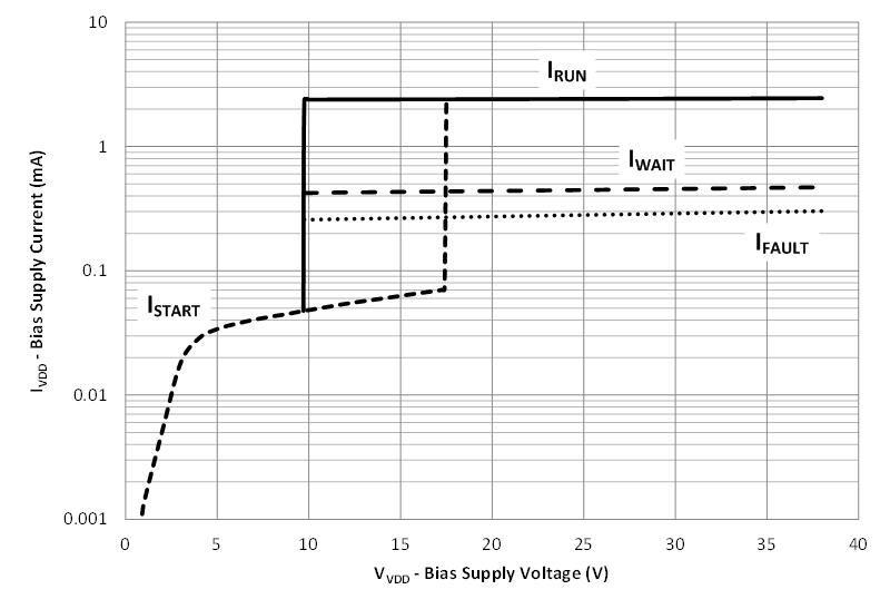
UCC28780 char-IVDDtoVDD.gif
Figure 1. VDD Bias-Supply Current vs. VDD Bias-Supply Voltage
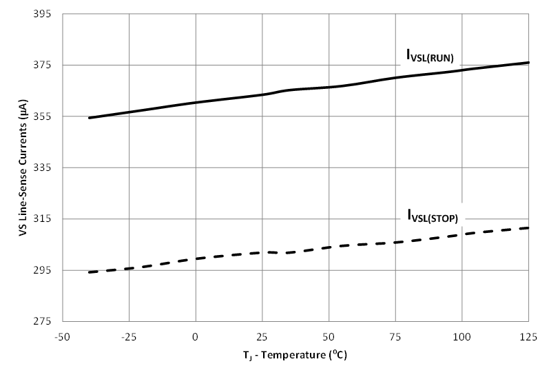
UCC28780 char-IVSLtoTJ.gif
Figure 3. VS Line-Sense Currents vs. Temperature
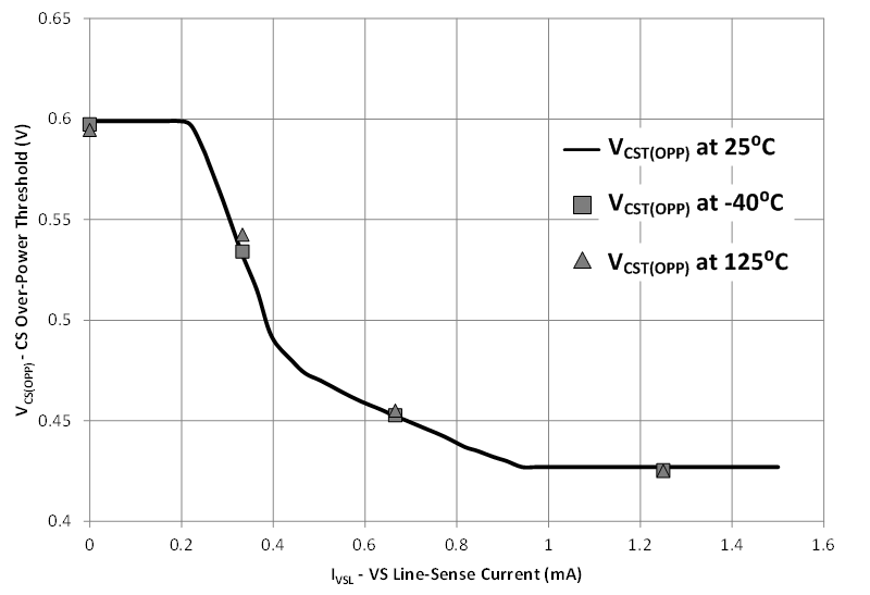
UCC28780 char-OPPtoIVSL.gif
Figure 5. CS Over-Power Threshold vs. VS Line-Sense Currents
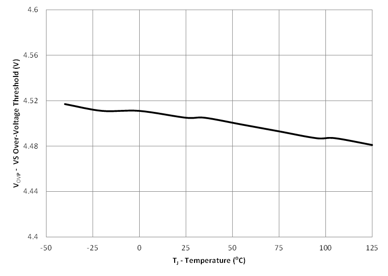
UCC28780 char-VOVPtoTJ.gif
Figure 7. VS Over-Voltage Threshold vs. Temperature
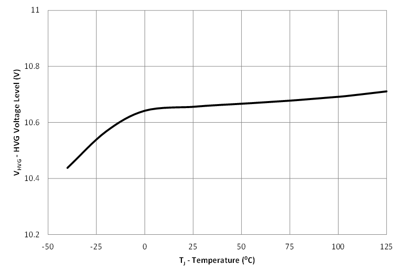
UCC28780 char-VHVGtoTJ.gif
Figure 9. HVG Voltage vs. Temperature
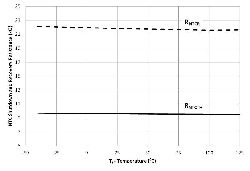
UCC28780 char-RNTCtoTJ.gif
Figure 11. NTC Thresholds vs. Junction Temperature
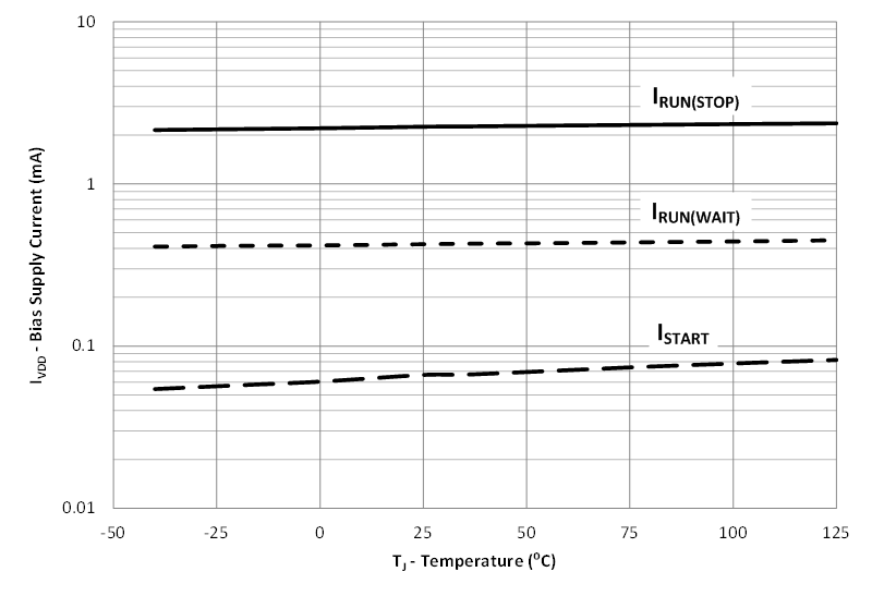
UCC28780 char-IVDDtoTJ.gif
Figure 2. VDD Bias-Supply Current vs. Junction Temperature
UCC28780 char-VCSTtoTJ.gif
Figure 4. Percentage Variation of Maximum and Minimum CS Thresholds vs. Temperature
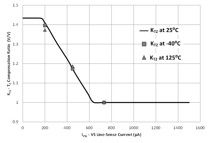
UCC28780 char-KTZtoIVSL.gif
Figure 6. tZ Compensation Ratio (KTZ) vs. VS Line-Sense Currents
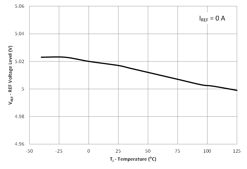
UCC28780 char-VREFtoTJ.gif
Figure 8. REF Voltage vs. Temperature
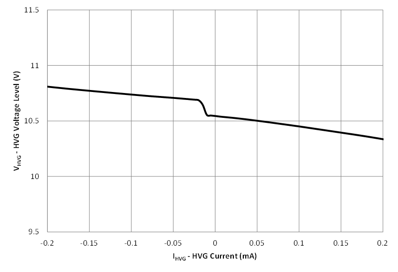
UCC28780 char-VHVGtoIHVG.gif
Figure 10. HVG Voltage vs. HVG Current