SNOAA68 June 2021 LMG3410R050 , LMG3410R070 , LMG3410R150 , LMG3411R050 , LMG3411R070 , LMG3411R150 , LMG3422R030 , LMG3422R050 , LMG3425R030 , LMG3425R050 , LMG3522R030-Q1 , LMG3526R030
6 Achieving Reliable Design
For the reliable operation of a power converter, the device needs to stay within certain voltage and current ranges. The designer looks to the Safe Operating Area (SOA) curve(20) for the limits and assumes that designs within SOA limits will be reliable for long-term operation. Measurements for traditional SOA curves are conducted using single current-pulses with the FET biased in saturation. Pulse widths used are typically longer than 100 µs and the measured boundary is typically derated by 30–35% to provide extra margin.
Since traditional SOA curves are empirically determined, it is not clear how they will guide the reliable design of modern power supplies. Fast power FETs can switch in less than 10 ns, but need to carry higher switching current due to the fast slew rate(5). Traditional SOA curves do not take into account wearout and the resulting lifetime implications due to repetitive switching at these conditions.
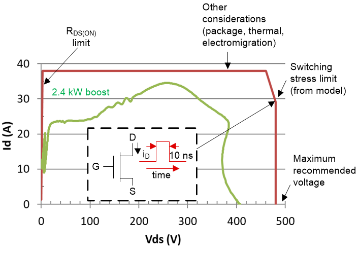
The switching SOA curve can guide the reliable design of modern power supplies by use of the switching stress model to calculate the switching stress limit. We have applied the model to generate the SOA curve in Figure 6-1 shown for the LMG3410R050. This switching stress boundary is calculated for 100-kHz operation with an ideal 10 ns drain-current pulse, illustrated in the inset, at each fixed value of VDS, where the drain current is defined as the current entering the drain terminal. The other boundaries of the curve are determined by different considerations. The figure also shows the switching locus curve of a hard-switched turn-on transition corresponding to 2.4 kW boost operation and switching time of 10 ns. Since the switching trajectory fits within the boundary, the part will operate reliably at this condition. In addition, there is margin, since the time at high voltage, where most wear out occurs, will be lower than 10 ns.
 Figure 6-1 SOA curve with use of
switching lifetime model to calculate the maximum switching stress limit. This
boundary is calculated for a 10-ns switching pulse and 100-kHz operation.
Applications with switching locus curves within the boundary will operate
reliably. The use of a linear VDS scale provides better resolution at
high voltage.
Figure 6-1 SOA curve with use of
switching lifetime model to calculate the maximum switching stress limit. This
boundary is calculated for a 10-ns switching pulse and 100-kHz operation.
Applications with switching locus curves within the boundary will operate
reliably. The use of a linear VDS scale provides better resolution at
high voltage.If either a measured or simulated switching locus curve is not available, the peak drain current during switching may be estimated using Equation 1. The peak drain current is calculated by adding the switched node capacitive charging current to the peak inductor current of a boost or buck converter at the time of FET turn-on of the hard-switching device:
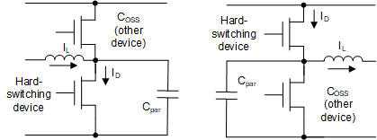
The drain slew rate for calculating the peak current (IDpeak) is estimated between 70 percent and 30 percent of the bus voltage and the switched node capacitance (CSW_node) is estimated as the sum of the overlap capacitance of the PCB (Cpar) and output capacitance COSS of the other GaN device in the half-bridge. The method is applicable for both buck and boost topologies, as shown in Figure 6-2.

Figure 6-2 The calculation of drain current while switching (Equation 1) is valid for both boost and buck topologies, for the hard-switching device. The capacitance at the switched node is the sum of the PCB overlap capacitance and the COSS of the other device in the half-bridge.