SPRACN9E september 2022 – may 2023 AM67 , AM67A , AM68 , AM68A , AM69 , AM69A , DRA829J , DRA829J-Q1 , DRA829V , DRA829V-Q1 , TDA4AEN-Q1 , TDA4VEN-Q1 , TDA4VM , TDA4VM-Q1
- 1
- Jacinto 7 LPDDR4 Board Design and Layout Guidelines
- Trademarks
- 1Overview
-
2LPDDR4 Board Design and Layout Guidance
- 2.1 LPDDR4 Introduction
- 2.2 LPDDR4 Device Implementations Supported
- 2.3 LPDDR4 Interface Schematics
- 2.4 Compatible JEDEC LPDDR4 Devices
- 2.5 Placement
- 2.6 LPDDR4 Keepout Region
- 2.7 Net Classes
- 2.8 LPDDR4 Signal Termination
- 2.9 LPDDR4 VREF Routing
- 2.10 LPDDR4 VTT
- 2.11 CK and ADDR_CTRL Topologies
- 2.12 Data Group Topologies
- 2.13 CK and ADDR_CTRL Routing Specification
- 2.14 Data Group Routing Specification
- 2.15 Channel, Byte, and Bit Swapping
- 3LPDDR4 Board Design Simulations
- 4Revision History
2.3 LPDDR4 Interface Schematics
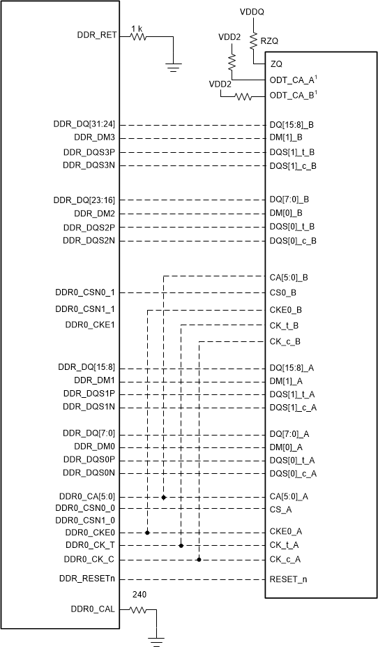
The LPDDR4 interface schematics vary, depending upon the number of ranks implemented. General connectivity is straightforward and consistent between the implementations. Figure 2-1 illustrates a 32-bit, single-rank LPDDR4 implementation. If dual rank is required, the additional chip select is included. Figure 2-2 illustrates a 32-bit, dual-rank LPDDR4 implementation. On select devices, 16-bit single-rank LPDDR4 implementation are support, see Figure 2-3.
Note: Though LPDDR4 SDRAMs pin out two
separate channels, independent channel use is not supported by this
processor.
 Figure 2-1 32-Bit, Single-Rank LPDDR4
Implementation
 Figure 2-2 32-Bit, Dual Rank LPDDR4
Implementation
 Figure 2-3 16-Bit, Single Rank LPDDR4
Implementation