SPRAD12A July 2022 – February 2023 F29H850TU , F29H859TU-Q1 , TMS320F280021 , TMS320F280021-Q1 , TMS320F280023 , TMS320F280023-Q1 , TMS320F280023C , TMS320F280025 , TMS320F280025-Q1 , TMS320F280025C , TMS320F280025C-Q1 , TMS320F280033 , TMS320F280034 , TMS320F280034-Q1 , TMS320F280036-Q1 , TMS320F280036C-Q1 , TMS320F280037 , TMS320F280037-Q1 , TMS320F280037C , TMS320F280037C-Q1 , TMS320F280038-Q1 , TMS320F280038C-Q1 , TMS320F280039 , TMS320F280039-Q1 , TMS320F280039C , TMS320F280039C-Q1 , TMS320F280040-Q1 , TMS320F280040C-Q1 , TMS320F280041 , TMS320F280041-Q1 , TMS320F280041C , TMS320F280041C-Q1 , TMS320F280045 , TMS320F280048-Q1 , TMS320F280048C-Q1 , TMS320F280049 , TMS320F280049-Q1 , TMS320F280049C , TMS320F280049C-Q1 , TMS320F28075 , TMS320F28075-Q1 , TMS320F28076 , TMS320F28374D , TMS320F28374S , TMS320F28375D , TMS320F28375S , TMS320F28375S-Q1 , TMS320F28376D , TMS320F28376S , TMS320F28377D , TMS320F28377D-EP , TMS320F28377D-Q1 , TMS320F28377S , TMS320F28377S-Q1 , TMS320F28378D , TMS320F28378S , TMS320F28379D , TMS320F28379D-Q1 , TMS320F28379S , TMS320F28384D , TMS320F28384D-Q1 , TMS320F28384S , TMS320F28384S-Q1 , TMS320F28386D , TMS320F28386D-Q1 , TMS320F28386S , TMS320F28386S-Q1 , TMS320F28388D , TMS320F28388S , TMS320F28P550SG , TMS320F28P550SJ , TMS320F28P559SG-Q1 , TMS320F28P559SJ-Q1 , TMS320F28P650DH , TMS320F28P650DK , TMS320F28P650SH , TMS320F28P650SK , TMS320F28P659DH-Q1 , TMS320F28P659DK-Q1 , TMS320F28P659SH-Q1
- Abstract
- Trademarks
- 1 Introduction
- 2 SysConfig
- 3 Time-Base (TB) Submodule
- 4 Counter-Compare (CC) and Action-Qualifier (AQ) Submodules
- 5 Deadband (DB) Submodule
- 6 Verifying the Output
- 7 Trip-Zone (TZ) and Digital Compare (DC) Submodules
- 8 Event-Trigger (ET) Submodule
- 9 Global Load
- 10Summary
- 11References
- 12Revision History
5.1 Setting up Signal Pairs
For this use-case, all three ePWM modules are set up for active high complementary signals. Meaning ePWMxA remains as is with a rising edge delay (RED) and ePWMB has the same source signal as ePWMA, but it is inverted with a falling edge delay (FED) instead of a rising edge delay. #FIG_EBV_FCV_4TB illustrates these two signals.
In order to set up these signal pairs, utilize the deadband submodule as it allows you to apply this scheme of outputs along with many other signal pairs.
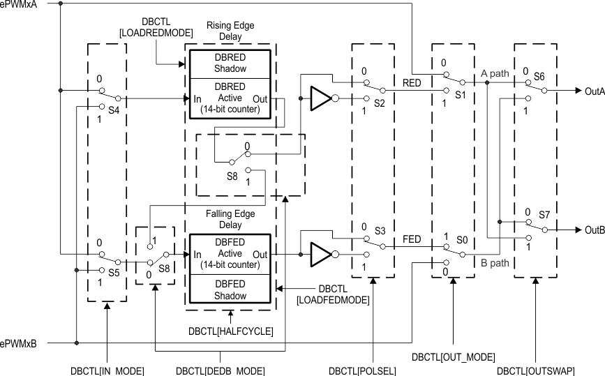
 Figure 5-2 Configuration Options for the
Deadband Submodule
Figure 5-2 Configuration Options for the
Deadband SubmoduleTo begin, take a look at the deadband submodule, which is essentially a set of switches that work together to achieve the desired output. S4 and S5 decide what the source signal is for the rest of the submodules: ePWMA or ePWMB. Since you want the same source signal for both resulting ePWMA and ePWMB outputs, set both switches to the ePWMA input. Next is S8, which is responsible for deciding which of the outputs will have RED and FED or both applied to it. Only one channel, either A or B, can have both RED and FED.
For this case, ePWMA will have RED and ePWMB will have FED so the switch is set to the zero position. Since ePWMB is inverted, S3 is in the 1 position, while S2 remains in the 0 position. The deadband module is being utilized, so S0 and S1 are both set to 1. The last step is deciding whether to swap the current outputs. For this use-case, leave S7 and S6 as-is, meaning the current setup is what is applied and not the swapped output versions.
#GUID-276A33C6-E402-4F9D-93A1-ED4D868F8241 shows this configuration within SysConfig. By pressing the ‘SETUP THE DEAD-BAND MODULE’ button next to the ‘Active High Complementary’ option, the SysConfig tool automatically sets up the module in the correct way to achieve active high complementary pairs.
In order to calculate the required dead-band rising edge delay (DBRED) and dead-band falling edge delay (DBFED), the below calculations are done:
Re-arrange the equation to find the value of DBRED, which is the value needed:
The period of the time-base clock is known from prior equations done in this application report:
// EPWM 1 (the code is the same for EPWM2 and EPWM3, except for the base address)
EPWM_setDeadBandDelayPolarity(myEPWM1_BASE, EPWM_DB_FED, EPWM_DB_POLARITY_ACTIVE_LOW);
EPWM_setDeadBandDelayMode(myEPWM1_BASE, EPWM_DB_RED, true);
EPWM_setRisingEdgeDelayCount(myEPWM1_BASE, 20);
EPWM_setDeadBandDelayMode(myEPWM1_BASE, EPWM_DB_FED, true);
EPWM_setFallingEdgeDelayCount(myEPWM1_BASE, 20);