SPRAD20 March 2022 AM2631 , AM2631-Q1 , AM2632 , AM2632-Q1 , AM2634 , AM2634-Q1
- Trademarks
- 1Introduction
-
2A Step-by-Step Guide to Running a Traction
Inverter
- 2.1 Create Real Time Debug Interface
- 2.2 Configure Control Peripheral and ADC Interrupt With Sysconfig
- 2.3 Configure Gate Driver Interface With MSPI
- 2.4 Get Samples From ADC and Read Samples Via CCS
- 2.5 Generate Space Vector PWM and Drive Motor in Open Loop
- 2.6 Close Current Loop With Mock Speed
- 2.7 Add Software Resolver to Digital Converter
- 2.8 Close Speed Loop With Rotor Speed
- 3A Brief Guide to Code Migration
- 4Summary
- 5References
2.2.1 Generate PWM for Time Reference
The PWM module of AM263x inherited features from TI classic C28 controllers. With a unique XBAR architecture of AM263x, its ADC SOC triggers are able to trigger not only ADC events but also various of other events like DMA. This part will give some details on how to synchronize PWM modules and how to configure PWM modules to trigger ADC and DMA. More details can be found in Technical Reference Manual.
Figure 2-18 presents a summary of ePWM7, which is used to trigger DMA for resolver excitation signal updating at 200 kHz via DAC. There are couple tabs available for configuration. But, for the DMA trigger purpose, there are only three tabs to be updated.
- EPWM Time Base
- EPWM Action Qualifier
- EPWM Event-Trigger
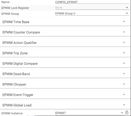 Figure 2-18 A Summary of EPWM7
Configuration
Figure 2-18 A Summary of EPWM7
ConfigurationFigure 2-19 shows details on Time Base. EPWM7 is configured as 200 kHz, Up-Count, and following Sync Out Pulse from ePWM0. It is worth attention that peripherals are operated at 200 MHz while R5F cores are running at 400 MHz.
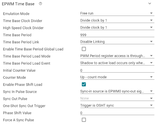 Figure 2-19 EPWM7 Time Base
Configuration
Figure 2-19 EPWM7 Time Base
ConfigurationFigure 2-20 shows details on Event Trigger. The key contents are listed below. ePWM7 is to generate two triggers, ADC SOCA and SOCB. The two triggers are from different source events The one related to CMPA is configured in the Counter Compare tab as shown in Figure 2-21.
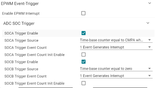 Figure 2-20 EPWM7 Event Trigger
Configuration
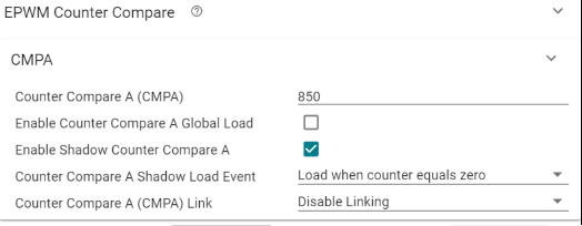 Figure 2-21 EPWM7 Counter Compare
Configuration
Figure 2-21 EPWM7 Counter Compare
ConfigurationEPWM0 is used as Phase A of traction inverter. All EPWM channels are synchronized to EPWM0. It is configured as 10 kHz, Up-Down Count, No Sync In, Sync Out and ADC SOC trigger at counter zero as shown by Figure 2-22 and Figure 2-23.
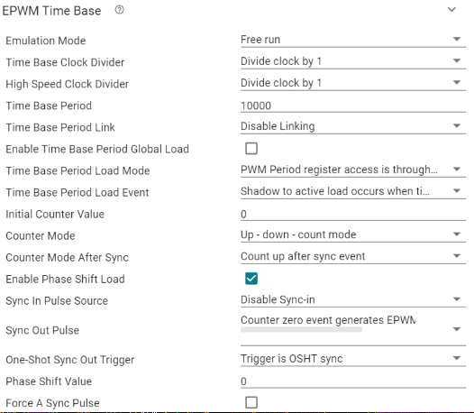 Figure 2-22 EPWM0 Time Base
Configuration
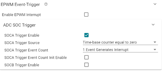 Figure 2-23 EPWM0 Event Trigger
Configuration
Figure 2-23 EPWM0 Event Trigger
ConfigurationDead-Band of EPWM0 is configured as Figure 2-24. Delay value of 200 indicates 1000 ns because of the 200 MHz peripherals clock.
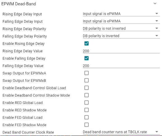 Figure 2-24 EPWM0 Dead-Band
Configuration