TIDUEM8B March 2019 – February 2021
2.3.2.3 Background Process
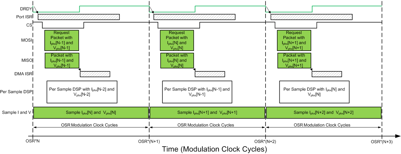
Figure 2-10 shows the different events that occur when sampling voltage and current, where the items in olive green are done by the hardware settings and not the test software.
 Figure 2-10 Voltage and Current Sampling Events
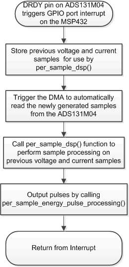
To go over the process mentioned in Figure 2-10, new current samples for each phase are ready every OSR, or 512 for this design, modulation clock cycles. Suppose the most recently ready phase current and voltage samples from the ADS131M04 device corresponds to the Nth – 1 current and voltage sample, or Iphx[N – 1] and Vphx[N – 1]. Once new samples are ready, the DRDY pin is asserted low by the ADS131M04. The falling edge on the DRDY pin on the ADS131M04 causes a GPIO port interrupt on the MSP432 MCU, which triggers the Port ISR on the MSP432 MCU. The background process is run within the Port ISR. Figure 2-11 shows the background process, which mainly deals with timing critical events in the test software.
 Figure 2-11 Background Process
In the background process, the previously-obtained voltage samples (Vphx[N – 2]) and previously obtained current samples (Iphx[N – 2]) are stored so that they can be used later by the per_sample_dsp function, which is responsible for updating the intermediate dot product quantities used to calculate metrology parameters. After the previously obtained voltage and current samples are stored, communication to the ADS131M04 is enabled by asserting the chip select signal low. The DMA is then configured to both send a request for the newest current and voltage samples (Iphx[N – 1] and Vphx[N – 1]) of the ADS131M04 device and also to receive the data packet response from the ADS131M04. The request and reception of the current samples is done automatically by the DMA module instead of it being done by the software.
Figure 2-12 shows the packet that is transmitted by the DMA of the MSP432 MCU and the response packet from the ADS131M04 that is received and assembled by the DMA as well. The transmission and reception packets contain six words, where each word is three bytes long.
 Figure 2-12 ADS131M04 ADC Sample Request Packet
When requesting the ADC data from the ADS131M04 device, the first word that has to be sent to the ADS131M04 is the command word. Since the test software does not need to change the settings of the ADS131M04 or read any registers during typical ADC sample readouts, a NULL command is sent to the ADS131M04, which allows you to get the ADC samples from the ADS131M04 without changing the state of the device. The actual size of the null command is 16-bits; however, since 24-bit words are used, the 16-bit command must be padded with an extra value of 0x00 at the end of the command. The NULL command word sent therefore has a value of 0x000000. While the MSP432 MCU is shifting out the command word, the MSP432 is simultaneously shifting in the response word to the command word of the previous packet. The response word to a NULL command is the contents of the STATUS register. The contents of the STATUS register is not used in this design so the first word received from the ADS131M04 is ignored.
After writing the command word, it is necessary for a dummy write to be performed for each byte that is to be read. The dummy byte write is necessary to enable the SPI clock, which is necessary to read a byte from the ADS131M04 device. For each dummy byte write, a value of 0x00 is written to the SPI transmit register for EUSCIB0. Immediately after writing the command byte, writing three dummy bytes allows the MSP432 MCU to receive the 3-byte ADC value from channel 0 of the ADS131M04. Writing the next nine dummy bytes gets the ADC data for channel 1, channel 2, and channel 3, respectively. Finally, writing the next three dummy bytes gets the CRC word. The CRC word is 24-bits; however, note that the actual CRC is only 16-bits, which are placed in the most significant bits of the 24-bit word. As a result, when parsing the CRC word, the last byte is not needed (note though that the dummy write for this zero-padded byte must still be sent though for proper ADS131M04 operation).
Figure 2-12 shows that whenever the DMA has received the entire Iphx[N – 1] packet, the DMA ISR is automatically called. Within the ISR, the CRC is calculated over the five command and ADC words (15 bytes in total). This CRC calculation uses the CRC module of the MSP432 MCU. Since the CRC module works with an even number of bytes but there are a total of 15 bytes available, the CRC module is used for the first 14 bytes. The final CRC is calculated in software from the CRC module result and the 15th byte. Note that the software CRC calculation on the last byte is only necessary because the word size was selected to be three bytes in this design. If the word size was selected to be two bytes or four bytes instead, the software CRC calculation would not be needed since there would be an even number of bytes. Figure 2-13 shows the code snippet for calculating the CRC over 15 bytes by using the MSP432 CRC module and software.
 Figure 2-13 Code Snippet for Using the CRC Module of the MSP432 MCU for Calculating CRC Over an Odd Number of Bytes
Once the CRC has been calculated over the packet, it is compared to the CRC obtained in the packet sent from the ADS131M04. The sent CRC is parsed from bytes 16 and 17 of the ADS131M04 packet (byte 18, which is part of the CRC word, is zero-padded so it is not used in parsing). If the calculated CRC and the parsed CRC are equal, then the CRC check passes and the ADC data is parsed to get the values of the voltage and current samples at time N – 1. The parsed voltage and current samples are put in temporary buffers so that they are used the next time the per_sample_dsp function is called at the next interrupt. Before the DMA interrupt ends, the chip select line is pulled back high again to properly reset the ADS131M04 communication before the next time current samples are ready from the ADS131M04.
In parallel to receiving the newest current samples from the ADS131M04 using the DMA, the ADS131M04 is currently sampling the next voltage (Vphx[N]) and current samples (Iphx[N]) and the test software also performs per-sample processing on the last voltage (Vphx[N – 2]) and current samples (Iphx[N – 2] ) obtained from the ADS131M04. This per-sample processing is used to update the intermediate dot product quantities that are used to calculate the metrology parameters. After sample processing, the background process uses the "per_sample_energy_pulse_processing" for the calculation and output of energy-proportional pulses. Once the per_sample_energy_pulse_processing is completed, the test software exits from the port ISR.