SBAA532A February 2022 – March 2024 ADS1119 , ADS1120 , ADS1120-Q1 , ADS112C04 , ADS112U04 , ADS1130 , ADS1131 , ADS114S06 , ADS114S06B , ADS114S08 , ADS114S08B , ADS1158 , ADS1219 , ADS1220 , ADS122C04 , ADS122U04 , ADS1230 , ADS1231 , ADS1232 , ADS1234 , ADS1235 , ADS1235-Q1 , ADS124S06 , ADS124S08 , ADS1250 , ADS1251 , ADS1252 , ADS1253 , ADS1254 , ADS1255 , ADS1256 , ADS1257 , ADS1258 , ADS1258-EP , ADS1259 , ADS1259-Q1 , ADS125H01 , ADS125H02 , ADS1260 , ADS1260-Q1 , ADS1261 , ADS1261-Q1 , ADS1262 , ADS1263 , ADS127L01 , ADS130E08 , ADS131A02 , ADS131A04 , ADS131E04 , ADS131E06 , ADS131E08 , ADS131E08S , ADS131M02 , ADS131M03 , ADS131M04 , ADS131M06 , ADS131M08
- 1
- Abstract
- Trademarks
- 1Bridge Overview
- 2Bridge Construction
- 3Bridge Connections
- 4Electrical Characteristics of Bridge Measurements
- 5Signal Chain Design Considerations
-
6Bridge Measurement Circuits
- 6.1 Four-Wire Resistive Bridge Measurement with a Ratiometric Reference and a Unipolar, Low-Voltage (≤5 V) Excitation Source
- 6.2 Six-Wire Resistive Bridge Measurement With a Ratiometric Reference and a Unipolar, Low-Voltage (≤ 5 V) Excitation Source
- 6.3 Four-Wire Resistive Bridge Measurement With a Pseudo-Ratiometric Reference and a Unipolar, High-Voltage (> 5 V) Excitation Source
- 6.4 Four-Wire Resistive Bridge Measurement with a Pseudo-Ratiometric Reference and Asymmetric, High-Voltage (> 5 V) Excitation Source
- 6.5 Four-Wire Resistive Bridge Measurement With a Ratiometric Reference and Current Excitation
- 6.6 Measuring Multiple Four-Wire Resistive Bridges in Series with a Pseudo-Ratiometric Reference and a Unipolar, Low-Voltage (≤5V) Excitation Source
- 6.7 Measuring Multiple Four-Wire Resistive Bridges in Parallel Using a Single-Channel ADC With a Ratiometric Reference and a Unipolar, Low-Voltage (≤ 5 V) Excitation Source
- 6.8 Measuring Multiple Four-Wire Resistive Bridges in Parallel Using a Multichannel ADC With a Ratiometric Reference and a Unipolar, Low-Voltage (≤ 5 V) Excitation Source
- 7Summary
- 8Revision History
5.2.2 Calculating NFC for a Bridge Measurement System
As described in Section 4.1, a bridge sensitivity of 2 mV/V and VEXCITATION = 5 V yields a maximum bridge output signal of 10 mV. Furthermore, the minimum weight measured by a weigh scale is zero, resulting in a minimum bridge output signal of 0 V. Therefore, the bridge output signal range is 0 to 10 mV, which is significantly smaller than the FSR of most ADCs even at the highest gain. For example, the ADS1235 FSR at a gain of 128 V/V was given as ±39 mV in the previous section. As such, a 0- to 10-mV input signal uses approximately one-eighth of the ADC FSR.
Substitute the system signal range for the ADC FSR in Equation 21 to calculate the expected noise-free resolution for a given bridge measurement design. Equation 26 returns the noise-free resolution for the 0- to 10-mV weigh scale signal range using the ADS1235 at gain = 128 V/V, ODR = 20 SPS, and the FIR filter (assuming a ratiometric 5-V VREF):
Applying the result of Equation 26 to Equation 24 yields a new value for NFC shown in Equation 27:
Regardless of the construction of the measurement system, this noise analysis yields the noise floor of the final system. Moreover, the results from Equation 27 help determine if the ADC is sufficient to meet the target design specifications. If the NFC value is insufficient, selecting a different measurement configuration, a higher-precision ADC, or averaging the data output may reduce the noise to an acceptable level.
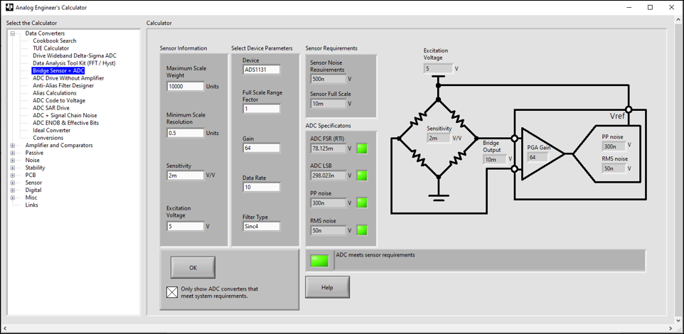
To help determine if an ADC can meet the target design specifications, use the Bridge Sensor + ADC tool in the Analog Engineer’s Calculator. Figure 5-5 introduces this tool and shows how it can be used. Enter the system requirements on the left and the tool returns available ADC options that meet the design goals. Converting voltage to bits, bits to effective resolution, or bits to noise-free resolution can also be performed.
 Figure 5-5 Bridge Sensor + ADC Tool in the Analog Engineer's Calculator