SBAA781 January 2026 ADS9224R , LMH6554 , OPA2320 , OPA2328 , OPA320 , OPA328 , OPA862 , THS2630 , THS4130 , THS4131 , THS4509 , THS4521 , THS4522 , THS4524 , THS4531 , THS4531A , THS4532 , THS4535 , THS4536 , THS4541 , THS4541-DIE , THS4541-Q1 , THS4551 , THS4552 , THS4561 , TMS320F28377D
Introduction
There is an increasing trend among analog-to-digital converters (ADC), including those embedded into microcontrollers such as the TMS320F2837xD family, to support the use of fully differential inputs to maximize product performance. This document aims to demonstrate the performance improvements and therefore importance of using a fully differential amplifier (FDA) to convert a single ended signal into a differential signal to drive a differential ADC compared to a discrete dual-channel operational amplifier (such as OPA2328 or OPA2320) through the laboratory analysis of multiple specifications. The focus specifications evaluated include even order harmonics (HD2, HD4), total harmonic distortion (THD), signal-to-noise ratio (SNR), and effective number of bits (ENOB). A summary of additional features including output common mode control, power consumption, ability for active filtering, ease of use, design size, and high input impedance are also derived.
Executive Summary
For a quick reference table summarizing the results of the following document, please refer to Table 1 for an executive summary.
| Specifications | Dual Operational Amplifier | Fully Differential Amplifier | Notes |
|---|---|---|---|
| Output Common Mode Control | ✓ | FDAs offer an integrated VOCM pin that allows for output common mode control independent of the input common mode, which is not available in a discrete design and has to be handled with careful consideration, especially when in a non-inverting configuration | |
| Solution Size and Complexity | ✓ | WQFN 10-Pin (RUN) is the industry's smallest FDA package, and does not require an external DC bias voltage for smallest design size | |
| Harmonic Distortion, CMRR | ✓ | Integrated FDA architecture offers improved CMRR and even-order harmonic distortion (HD2, 4) performance due to device matching and common-mode rejection princples | |
| Large Signal Step / Phase Delay | ✓ | FDAs can handle larger gain values with faster settling times compared to a dual op amp to ensure settling within ½ LSB of an ADC acquisition time | |
| Quiescent Current (Power Consumption) | ✓ | FDAs typically operate at the same or lower power for one channel of an op amp, further improved when considering the necessity for 2 op amp channels | |
| Active Filtering | ✓ | FDAs can support active filtering on the device in a single stage, eliminating the need for additional components to add a filter | |
| High Input Impedance | ✓ | An FDA input impedance is always resistive and cannot support high input impedance without the addition of a buffer amplifier on each input | |
| Cost | ✓ | Fully differential amplifiers, especially with the new THS4535, can be equivalent or lower cost than dual op amps |
Circuit Configuration and Implementation
Figure 1 shows the circuit configuration when using a dual channel operational amplifier to drive the inputs of a differential ADC. Notice that when using a dual channel op amp in a non-inverting configuration for high impedance, typically there are two reference voltages required because of the dependencies on the input and output bias voltages of each amplifier stage to adjust the final output common mode. This typically requires purchasing an additional IC, a low-noise voltage inverter such as LM27761, to produce a negative dc bias resulting in a larger design size and greater system cost.
Subsequently, Figure 2 showcases the circuit configuration for a fully differential amplifier when driving a differential ADC, which does not typically require any external reference voltage. The common-mode voltage pin on the FDA can be tied directly to the reference voltage output of the ADC, with no additional bias voltage handling due to the internal error loop amplifier integrated within an FDA.
 Figure 1 Dual Operational Amp Configuration for Differential Output Drive
 Figure 2 Fully Differential Amplifier Configuration for Differential Output Drive
Device Architecture Comparison
The two devices that have been selected for comparison and analysis are the OPA2328 operational amplifier and THS4536 fully differential amplifier. With similar process technologies, bandwidth performance, and precision specifications, they would be comparable devices to select for ADC drive when looking for a high DC precision design.
This table also serves to demonstrate the difference in quiescent current in a fully differential amplifier compared to a dual channel op amp when both are designed on a CMOS process. At 7.6mA for both channels of the OPA2328 compared to 4.7mA for just one THS4536, a fully differential amplifier shows a 14.5mW or a 38% reduction when using a 5V supply.
| Specifications | OPA2328 | THS4536 |
|---|---|---|
| Architecture | Operational Amplifier | Fully Differential Amplifier |
| Process | CMOS | CMOS |
| Supply Voltage Range (V) | 2.2 – 5.5 | 2.7 – 5.5 |
| Gain Bandwidth Product (MHz) | 40 | 80 |
| Slew Rate (V/μs) | 30 | 57 |
| Voltage Noise at 1kHz (nV/√Hz) | 6.1 | 4.3 |
| CMRR (typ) (dB) | 120 | 140 |
| Quiescent Current (total) (mA) | 7.6 | 4.7 |
| Rail to Rail | In, Out | In to V-, Out |
| Offset Voltage (25°C, max) (mV) | 0.05 | 0.05 |
| Offset Voltage Drift (typ) (μV/°C) | 0.15 | 0.8 |
| Cost | $$ | $ |
Total Harmonic Distortion (THD)
Total harmonic distortion is defined as the measure of unwanted frequencies (harmonics) that are added into an ideal signal (8). Ideally, the lower the THD, the better. The linearity of an amplifier can be quantified in terms of its THD performance, with a general rule of thumb that an engineer must select an amplifier at least 10 dB better than the ADC in the frequency range of interest. For FDAs, the even-order harmonics are ideally reduced in a differential signal path, resulting in a lower total harmonic distortion (5). Figure 4 demonstrates part of this principle as the total harmonic distortion is lower for the THS4536 compared to OPA2328 when driving multiple different input frequencies for a SAR 16-bit, 1MSPS ADC (ADS9224R).
 Figure 3 HD2 and HD4 vs. Input Frequency
 Figure 4 Total Harmonic Distortion vs. Input Frequency (1MSPS)
Large Signal Step and Phase Delay
Phase delay is defined as the difference in the phase of the positive and negative input terminals to a differential ADC. To obtain maximum performance and accuracy from the ADC, the phase and amplitude components of the input signals into the ADC should be ideally matched ensuring that the even order harmonics (2nd and 4th order) are minimally affected, signal bandwidths are optimized, and settling errors are reduced. When in a dual op amp configuration, the gain is typically increased on the 1st stage amplifier which causes the amplifier to slow compared to the 2nd stage amplifier which exacerbates the gain and phase imbalance. Comparatively, an FDA's architecture inherently has excellent output balance as the input stages are handled in parallel including the application of gain, resulting in minimal phase delay. These principles along with noise performance and settling errors can be demonstrated through the effective number of bits (ENOB) of performance from the ADC.
 Figure 5 ENOB vs. Input Frequency
Spectral Noise
The impact of an external amplifier's impact on system noise can be a complex analysis; however, the general guiding principle is to select an amplifier that is equal to or lower than the overall system noise at the desired gain level. For an in-depth discussion of how to calculate the effective noise bandwidth (ENBW) of an ADC, and the impact of an external amplifier, consider reference 9 Fundamentals of Precision ADC Noise Analysis Chapters 2 and 3. For short term consideration and evaluation, Figure 6 demonstrates the Fast Fourier Transform (FFT) vs. Frequency graph of spectral noise of the OPA2328 and THS4536 driving the ADS9224S with a 1kHz signal, showing that the THS4536 has lower flicker noise. The larger the flicker (1/f) noise and the further out in frequency the crossover occurs between flicker and broadband noise, the more noise the ADC will sample allowing for a degraded output code result and reduced effective bandwidth of the ADC. Additionally Signal to Noise Ratio (or SNR), which is a measure of the strength of an input signal compared to unwanted noise, can be used to showcase the performance benefits of the THS4536 when driving the ADC.
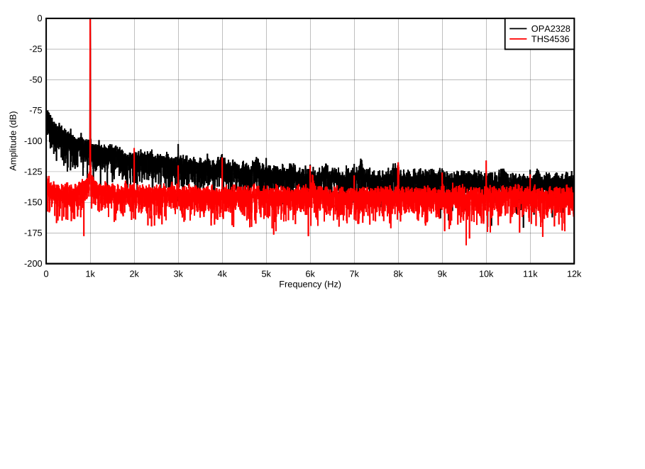 Figure 6 FFT vs. Frequency
 Figure 7 SNR vs. Frequency (1MSPS)
Conclusion
Fully differential amplifiers offer many signal chain improvements due to their integrated architecture and inherent differential signal properties. For the same or lower power consumption, an engineer can expect to see the smallest impact to SNR, lowest THD, largest ENOB, reduced design size, integrated output common mode control, and the ability to add an active filter onto the same component all with a simple to use, lower cost device. By selecting the correct FDA for an ADC, it ensures that maximum performance is realized from the ADC and therefore subsequent final system, with ease of implementation.
Popular ADCs and FDA Recommendations
| Analog to Digital Converter (ADC) | ADC Architecture | Suggested Fully Differential Amplifier Driver |
|---|---|---|
| ADS1675 | ∆Σ, 24-bit, 4MSPS | LMH6551 |
| THS1209 | Pipeline, 12-bit, 8MSPS | THS4551 |
| ADS9224 | SAR, 16-bit, 3MSPS | THS4551 |
| ADS9327 | SAR, 16-bit, 5MSPS | THS4551 |
| ADS1278 | ∆Σ, 24-bit, 144kSPS | THS4536 |
| ADS127L11 | ∆Σ, 24-bit, 400kSPS | THS4536 |
| ADC3544 | SAR, 14-bit, 125MSPS | THS4541 |
| ADS1602 | ∆Σ, 16-bit, 2.5MSPS | THS4561 |
Additional References to Learn More
- Precision Labs Series: Fully Differential Amplifiers
- Designing a Front-End Circuit for Driving a Differential Input ADC
- Active Filter Design for Differential ADCs
- Fully Differential Amplifiers
- Carissa Slipp, Microwave Journal, Fully-Differential Amplifiers and Benefits When Driving ADCs
- Pairing ADC Drivers With Fully Differential Input ADCs for Wide Bandwidth Data Acquisition
- Has Distortion Got Your Amplifier Down? Get More Bandwidth!
- Maximizing Signal Chain Distortion Performance Using High Speed Amplifiers
- Fundamentals of Precision ADC Noise Analysis
- Common Design Challenges and Proper Use of Fully Differential Amplifiers (FDA)
- Fully Differential Online Calculator
- THS4536 Datasheet
Trademarks
All trademarks are the property of their respective owners.