SCEA065B November 2018 – March 2021 SN74AVC4T774 , SN74AXC1T45 , SN74AXC4T245 , SN74AXC4T774 , SN74AXC8T245 , SN74AXC8T245-Q1 , SN74AXCH1T45 , SN74AXCH4T245 , SN74AXCH8T245
2.5.3 Skew Performance
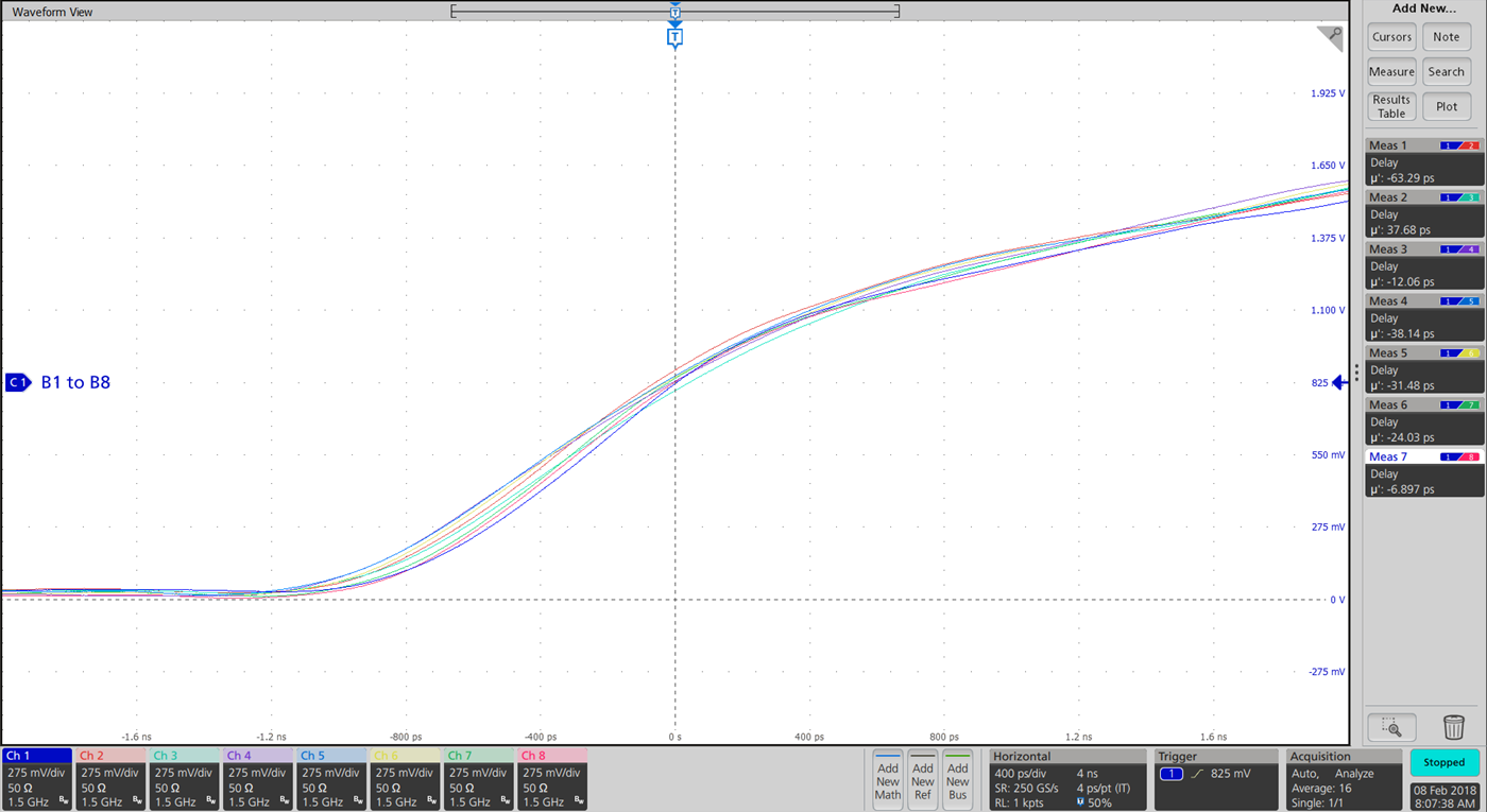
Output skew is defined as the difference between the propagation delay on the output channels which are driving equal loads with all the inputs arriving at the same time. It is particularly important in the RGMII interface where the high speed clock needs to synchronize the data on RX and TX lines with maximum allowed skew of 500 ps. See the RGMII Interface Timing Budgets application report. The output channel-to-channel skew for A-to-B direction rising-edge input under standard loading conditions is 104 ps as shown in Figure 2-14. The measurement was taken with 1.65 V Vcca, 3.3 V Vccb at 25°C. Similarly, under the same condition, the falling edge skew measurement is 127 ps.
 Figure 2-14 104 ps Channel-to-Channel Skew
for SN74AXC8T245