SLLA383A February   2018  – August 2022 SN65HVDA100-Q1 , SN65HVDA195-Q1 , TLIN1022-Q1 , TLIN1029-Q1 , TLIN2022-Q1 , TLIN2029-Q1 , TMS320F28P550SJ , TMS320F28P559SJ-Q1


  1.   Abstract
  2.   Trademarks
  3. 1Introduction
    1. 1.1 LIN Specification Progression
    2. 1.2 Workflow Concept
  4. 2Network Architecture
    1. 2.1 General Layout of the LIN Bus
    2. 2.2 Serial Communication Principles
    3. 2.3 Commander-Responder Principle
    4. 2.4 Message Frame Format
  5. 3Physical Layer Requirements
    1. 3.1 Bus Signaling Fundamentals
    2. 3.2 Pullup Values
    3. 3.3 Threshold Values
    4. 3.4 Bit-Rate Tolerance and Timing Requirements
    5. 3.5 Synchronization and Bit Sampling
    6. 3.6 Duty Cycle
  6. 4Filtering, Distance Limitations, Nodes on Bus
    1. 4.1 EMI and Signal Conditioning
    2. 4.2 ESD and Transients
    3. 4.3 Distance and Node Limitations
  7. 5LIN Transceiver Special Functions
    1. 5.1 Low-Power Modes
      1. 5.1.1 Sleep Mode
      2. 5.1.2 Standby Mode
    2. 5.2 Wakeup
      1. 5.2.1 Pin Wakeup
      2. 5.2.2 LIN Wakeup
      3. 5.2.3 Dominant Timeout
  8. 6Advantages and Disadvantages
  9. 7Conclusion
  10. 8Revision History

LIN Wakeup

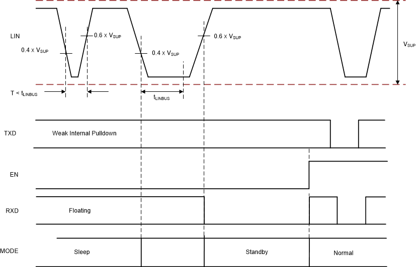
LIN wakeup is a request made on the LIN bus while the transceiver is in Sleep mode. This request is a specific pattern that the transceiver detects while monitoring the bus in the low-power mode. The pattern is a recessive-to-dominant transition where the dominant position is held for the specified amount of time. When the dominant pulse is held for the correct amount of time, the LIN transceiver transitions into Standby mode, and RXD is held low. Figure 5-1 shows a timing diagram of the procedure.
GUID-FDF2A254-8391-4225-8DAB-16CEB98F8023-low.gifFigure 5-1 LIN Wake-up Pattern