SLOA170B July 2012 – January 2021 DRV8242-Q1 , DRV8412 , DRV8424 , DRV8424E , DRV8425 , DRV8425E , DRV8426 , DRV8426E , DRV8428 , DRV8428E , DRV8434 , DRV8434E , DRV8436 , DRV8436E , DRV8701 , DRV8702-Q1 , DRV8702D-Q1 , DRV8703-Q1 , DRV8703D-Q1 , DRV8705-Q1 , DRV8706-Q1 , DRV8800 , DRV8801 , DRV8802 , DRV8802-Q1 , DRV8811 , DRV8812 , DRV8813 , DRV8814 , DRV8818 , DRV8821 , DRV8823 , DRV8823-Q1 , DRV8824 , DRV8824-Q1 , DRV8825 , DRV8828 , DRV8829 , DRV8832 , DRV8832-Q1 , DRV8833 , DRV8834 , DRV8840 , DRV8841 , DRV8842 , DRV8843 , DRV8844 , DRV8846 , DRV8848 , DRV8870 , DRV8874 , DRV8874-Q1 , DRV8876 , DRV8876-Q1 , DRV8880 , DRV8881 , DRV8885 , DRV8886 , DRV8889-Q1 , DRV8899-Q1 , DRV8935 , DRV8955
1.1 The Current Regulation Engine
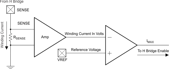
There are two possible implementations for a current regulation engine on the DRV88xx family of power stage devices: Internal or External VREF. Figure 1-1 depicts the typical analog block utilized to sample current information and disable the H Bridge accordingly. User must refer to respective device’s datasheet to learn whether the Analog Reference Voltage is internal or external to the device.
 Figure 1-1 Current Regulation Analog Block
The Current Regulation Block is continuously monitoring motor winding current by sampling the voltage across the SENSE resistor. The SENSE resistor is in series with the H Bridge, so the current flowing through the inductive load will be the same as across the resistor. The SENSE resistor is chosen to be as small as possible in order to minimize power losses. This makes the voltage drop across it proportionally small.
In order for the SENSE voltage drop to be properly compared with the reference voltage, an amplifier is put in place. Typical gains for this amplifier stage are 5, 8, and so forth. User must refer to the respective device’s datasheet to determine the amplifier’s gain.
The amplified voltage is then compared against the reference voltage. When the amplified SENSE resistor voltage is greater than the reference voltage, this signifies winding current is larger than the target current. This event is referred to as an ITRIP event and when this happens, the device’s logic disables the H Bridge and allows the current to decay through the internal structure. This process is repeated on a continuous basis thus obtaining a regulated current output.
An ITRIP event will generate an immediate H Bridge disablement as long as the H Bridge has been enabled for longer than the TBLANK period. In order to filter out spurious noise at the SENSE resistor, caused by H Bridge enablement, a small delay is put in place. During this delay, the SENSE resistor voltage is not sampled.