SLUS812E February 2008 – September 2025 TPS51200
PRODUCTION DATA
- 1
- 1 Features
- 2 Applications
- 3 Description
- 4 Pin Configuration and Functions
- 5 Specifications
-
6 Detailed Description
- 6.1 Overview
- 6.2 Functional Block Diagram
- 6.3
Feature Description
- 6.3.1 Sink and Source Regulator (VO Pin)
- 6.3.2 Reference Input (REFIN Pin)
- 6.3.3 Reference Output (REFOUT Pin)
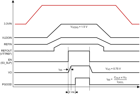
- 6.3.4 Soft-Start Sequencing
- 6.3.5 Enable Control (EN Pin)
- 6.3.6 Powergood Function (PGOOD Pin)
- 6.3.7 Current Protection (VO Pin)
- 6.3.8 UVLO Protection (VIN Pin)
- 6.3.9 Thermal Shutdown
- 6.3.10 Tracking Start-up and Shutdown
- 6.3.11 Output Tolerance Consideration for VTT DIMM Applications
- 6.3.12 REFOUT (VREF) Consideration for DDR2 Applications
- 6.4 Device Functional Modes
- 7 Application and Implementation
- 8 Device and Documentation Support
- 9 Revision History
- 10Mechanical, Packaging, and Orderable Information
6.3.10 Tracking Start-up and Shutdown
The TPS51200 also supports tracking start-up and shutdown when the EN pin is tied directly to the system bus and not used to turn on or turn off the device. During tracking start-up, VO follows REFOUT once REFIN voltage is greater than 0.39V. REFIN follows the rise of VDDQ rail through a voltage divider. The typical soft-start time (tSS) for the VDDQ rail is approximately 3ms, however it may vary depending on the system configuration. The soft-start time of the VO output no longer depends on the OCL setting, but it is a function of the soft-start time of the VDDQ rail. PGOOD is asserted 2ms after VVO is within ±20% of REFOUT. During tracking shutdown, the VO pin voltage falls following REFOUT until REFOUT reaches 0.37V. When REFOUT falls below 0.37V, the internal discharge MOSFETs turn on and quickly discharge both REFOUT and VO to GND. PGOOD is deasserted when VO is beyond the ±20% range of REFOUT. Figure 6-2 shows the typical timing diagram for an application that uses tracking start-up and shutdown.
 Figure 6-1 Typical Timing Diagram for S3 and Pseudo-S5 Support
 Figure 6-2 Typical Timing Diagram of Tracking Start-up and Shutdown