SLUS812E February 2008 – September 2025 TPS51200
PRODUCTION DATA
- 1
- 1 Features
- 2 Applications
- 3 Description
- 4 Pin Configuration and Functions
- 5 Specifications
-
6 Detailed Description
- 6.1 Overview
- 6.2 Functional Block Diagram
- 6.3
Feature Description
- 6.3.1 Sink and Source Regulator (VO Pin)
- 6.3.2 Reference Input (REFIN Pin)
- 6.3.3 Reference Output (REFOUT Pin)
- 6.3.4 Soft-Start Sequencing
- 6.3.5 Enable Control (EN Pin)
- 6.3.6 Powergood Function (PGOOD Pin)
- 6.3.7 Current Protection (VO Pin)
- 6.3.8 UVLO Protection (VIN Pin)
- 6.3.9 Thermal Shutdown
- 6.3.10 Tracking Start-up and Shutdown
- 6.3.11 Output Tolerance Consideration for VTT DIMM Applications
- 6.3.12 REFOUT (VREF) Consideration for DDR2 Applications
- 6.4 Device Functional Modes
- 7 Application and Implementation
- 8 Device and Documentation Support
- 9 Revision History
- 10Mechanical, Packaging, and Orderable Information
7.5.3 Thermal Design Considerations
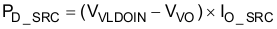
Because the TPS51200 is a linear regulator, the VO current flows in both source and sink directions, thereby dissipating power from the device. When the device is sourcing current, the voltage difference shown in Equation 5 calculates the power dissipation.
In this case, if the VLDOIN pin is connected to an alternative power supply lower than the VDDQ voltage, overall power loss can be reduced. During the sink phase, the device applies the VO voltage across the internal LDO regulator. Equation 6 calculates he power dissipation, PD_SNK can be calculated by .

Because the device does not sink and source current at the same time and the I/O current may vary rapidly with time, the actual power dissipation should be the time average of the above dissipations over the thermal relaxation duration of the system. The current used for the internal current control circuitry from the VIN supply and the VLDOIN supply are other sources of power consumption. This power can be estimated as 5mW or less during normal operating conditions and must be effectively dissipated from the package.
Maximum power dissipation allowed by the package is calculated by Equation 7.

where
- TJ(max) is 125°C
- TA(max) is the maximum ambient temperature in the system
- θJA is the thermal resistance from junction to ambient
Because Equation 7 demonstrates the effects of heat spreading in the ground plane, use it as a guideline only. Do not use Equation 7 to estimate actual thermal performance in real application environments.
In an application where the device is mounted on PCB, TI strongly recommends using ψJT and ψJB, as explained in the section pertaining to estimating junction temperature in the Semiconductor and IC Package Thermal Metrics application report, SPRA953. Using the thermal metrics ψJT and ψJB, as shown in the Section 5.4 table, estimate the junction temperature with corresponding formulas shown in Equation 8. The older θJC top parameter specification is listed as well for the convenience of backward compatibility.


where
- PD is the power dissipation shown in Equation 5 and Equation 6
- TT is the temperature at the center-top of the IC package
- TB is the PCB temperature measured 1mm away from the thermal pad package on the PCB surface (see Figure 7-13).
Both TT and TB can be measured on actual application boards using a thermo-gun (an infrared thermometer). For more information about measuring TT and TB, see the application report Using New Thermal Metrics (SBVA025).
 Figure 7-12 Recommended Land Pad Pattern
 Figure 7-13 Package Thermal Measurement