SLVA275C january 2010 – may 2023 UCD9081
- Abstract
- Trademarks
- 1Introduction
- 2Hardware
- 3Software
-
4User Configuration
- 4.1 Configuration Parameter Memory Map
- 4.2
Configuration Parameter Detail
- 4.2.1 GpDir
- 4.2.2 NegateEnablePolarity
- 4.2.3 SeqEventPending
- 4.2.4 SequenceEventParameters
- 4.2.5 SequenceEventLink
- 4.2.6 SequenceEventData
- 4.2.7 DependencyMasks
- 4.2.8 UnderVoltageThresholds
- 4.2.9 OverVoltageThresholds
- 4.2.10 RampTime
- 4.2.11 OutOfRegulationWidth
- 4.2.12 UnsequenceTime
- 4.2.13 EnablePolarity
- 4.2.14 SaveRailLog
- 4.2.15 ReferenceSelect
- 4.2.16 LastUnusedSeq
- 4.2.17 IgnoreGlitchAlarms
- 4.2.18 IgnoreFlashErrorLog
- 4.2.19 Checksum
- 5Additional Considerations
- 6References
- 7Revision History
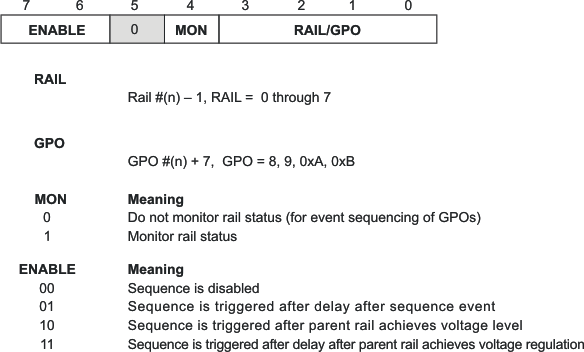
4.2.4 SequenceEventParameters
The SequenceEventParameters field in the configuration parameters specifies the rail identification, monitoring status, and sequencing options for each rail. The address map for these registers is as follows:
| Address | Size | Default Value | Description |
|---|---|---|---|
| 0xE080 | 1 | 0x50 | Rail 1 identification, monitoring status and sequencing options |
| 0xE081 | 1 | 0x51 | Rail 2 identification, monitoring status, and sequencing options |
| 0xE082 | 1 | 0x52 | Rail 3 identification, monitoring status, and sequencing options |
| 0xE083 | 1 | 0x53 | Rail 4 identification, monitoring status, and sequencing options |
| 0xE084 | 1 | 0x54 | Rail 5 identification, monitoring status, and sequencing options |
| 0xE085 | 1 | 0x55 | Rail 6 identification, monitoring status, and sequencing options |
| 0xE086 | 1 | 0x56 | Rail 7 identification, monitoring status, and sequencing options |
| 0xE087 | 1 | 0x57 | Rail 8 identification, monitoring status, and sequencing options |
| 0xE088 | 1 | 0x00 | GPO1 identification, sequencing options |
| 0xE089 | 1 | 0x49 | GPO2 identification, sequencing options |
| 0xE08A | 1 | 0x4A | GPO3 identification, sequencing options |
| 0xE08B | 1 | 0x4B | GPO4 identification, sequencing options |
The format of each register is as follows: