SLVAE30E February 2021 – March 2021 TPS1H000-Q1 , TPS1H100-Q1 , TPS1H200A-Q1 , TPS1HA08-Q1 , TPS25200-Q1 , TPS27S100 , TPS2H000-Q1 , TPS2H160-Q1 , TPS2HB16-Q1 , TPS2HB35-Q1 , TPS2HB50-Q1 , TPS4H000-Q1 , TPS4H160-Q1
- Trademarks
- 1Introduction
- 2Driving Resistive Loads
- 3Driving Capacitive Loads
- 4Driving Inductive Loads
- 5Driving LED Loads
- 6Appendix
- 7References
- 8Revision History
3.3.2 Inrush Current Mitigation
A simple example of a modeled capacitive load can be seen in Figure 3-5. This circuit shows a simplified model of a switch driving a 500mA DC load at 24V with a 10µF output capacitor. This example shows the cable as 100mΩ and 5µH:
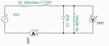 Figure 3-5 Uncontrolled Capacitor Charging Schematic
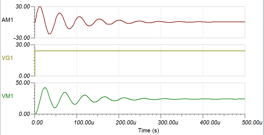 Figure 3-6 Uncontrolled Capacitor Charging Waveform
Figure 3-6 shows that an uncontrolled dV/dT leads to an inrush current that reaches nearly 30A with severe ringing. Without current limiting this is the quickest way to charge the capacitor, however for many systems this sort of inrush current is not acceptable and cannot be supported by the input power rail.
One option would be to find a way to limit this current while not impacting the system or causing the capacitor charging time to become too long. A simple solution would be for the designer to add a 12Ω current limiting resistor as seen in Figure 3-7.
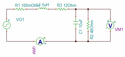 Figure 3-7 Series Resistance Capacitor Charging Schematic
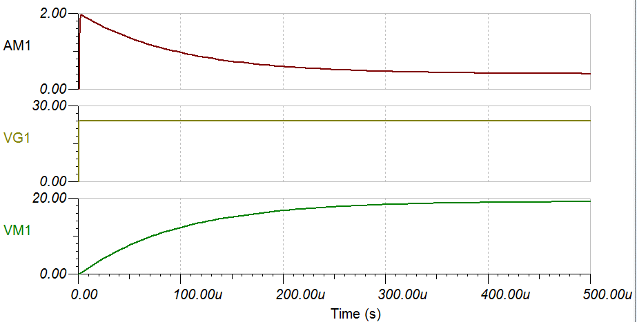 Figure 3-8 Series Resistance Capacitor Charging Simulation
The addition of a 12Ω current limiting resistor limits the peak current to less than 2A, but is not a viable solution due to the power dissipation and voltage drop over the additional 12-Ω resistance. With a 500mA DC load this adds 3W of additional power dissipation and a 6V drop over the resistor. This heat dissipation and voltage drop are not acceptable in the majority of applications.
Even for a relatively small 10µF load a better solution is needed. For larger capacitive loads these effects will be magnified further.
TI Smart High Side Switches are capable of limiting inrush current by linearly charging the capacitive load through current limiting. When charging a capacitor the Smart High Side Switch recognizes the over-current event and clamps the output current at an adjustable set point. Figure 3-9, shows where the TPS2H160-Q1 charges 470µF of capacitance with the current limit set to 1A:
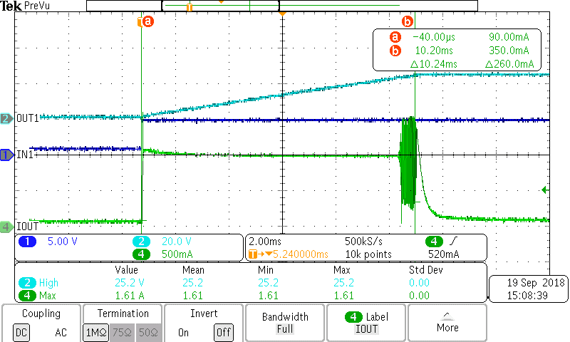 Figure 3-9 TPS2H160-Q1 Current Limiting at 1A
Now the capacitor charges fully without allowing the output current to exceed 1A and without adding significant DC series resistance to the system. Due to the FET heating up during this charging period some ringing occurs at the end because of the high temperature transition between the internal MOSFET modes of operation, however this poses no risk to the system due to the short transient length. The TPS2H160-Q1 has an on-resistance of only 160mΩ, so the same 500mA DC operating current means a power loss of only 40mW and a voltage drop of 80mV. These values are more acceptable for the system and will not cause unnecessary heat generation inside the module.
If the 1A inrush current is too significant the TPS2H160-Q1 allows the flexibility to further lower the current limit to 500mA as shown in Figure 3-10.
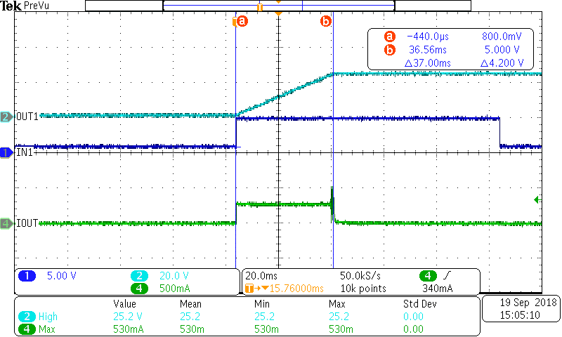 Figure 3-10 TPS2H160-Q1 Current Limiting at 500 mA
The voltage over the capacitor charges linearly with a constant current that never exceeds the set level. When taking into account the best way to limit inrush current, TI Smart High Side Switch current limiting provides a balanced solution for limiting inrush current while driving a capacitive load.