SLVAEP5A April 2020 – June 2021 LM3668 , TPS63000 , TPS63000-Q1 , TPS63001 , TPS63002 , TPS63010 , TPS63011 , TPS63020 , TPS63020-Q1 , TPS63021 , TPS63024 , TPS630241 , TPS630242 , TPS630250 , TPS630251 , TPS630252 , TPS63027 , TPS63030 , TPS63031 , TPS63036 , TPS63050 , TPS63051 , TPS63060 , TPS63061 , TPS63070 , TPS63802 , TPS63805 , TPS63806 , TPS63810 , TPS63811 , TPS63900 , TPS63901
3 Device Optimization
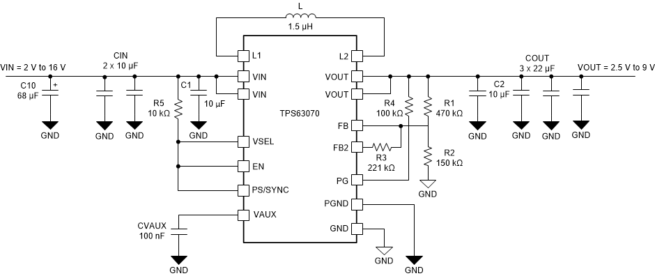
Figure 3-1 shows the circuit of a typical application of TPS63070. This circuit is used in this application note. The starting PCB layout concept is the recommended Webench layout for PCB built provided by Texas Instruments.
Please note that the Webench layout is not optimized for best EMI performance, but for the ability to place different size components.
 Figure 3-1 Typical Application of TPS63070
The Webench PCB layout is a two layer approach. All the planes, except the inductor ports, are kept on the top layer. The bottom layer consists of the inductor terminals and input and output planes. Optimizations can be done to the Webench layout in order to improve the radiated performance as follows:
- Minimizing hot planes: The area size of the nets corresponding to the input, output, inductor and other components connections should be kept as small as the design permits. Maximum area size should be assigned to the ground planes.
- Keeping traces entirely on one layer: Avoid as much as possible crossing between layers in the middle of a trace. This procedure reduces the number of vias and lowers the overall plane inductance.
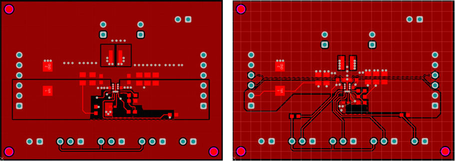
Figure 3-2 shows the top layers of the Webench layout (left) and the optimized layout (right). It highlights the minimized planes and the lack of cross layer talk.
 Figure 3-2 Top Layers of Webench Layout (left) Optimized Layout (right)
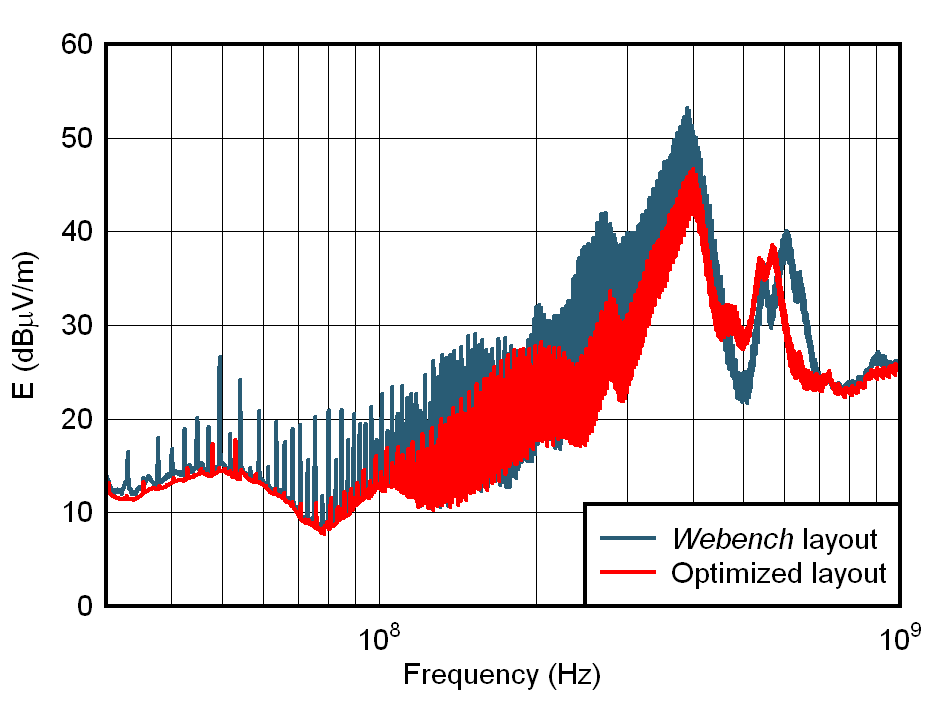
Figure 3-3 shows the benefits of the above mentioned improvements. The difference between the two measurements is significant and easily observable. Numerically, this difference can be as high as 10 dB at the most affected frequencies.
 Figure 3-3 Radiated EMI Response of the Webench Layout and the Optimized Layout