SLVAEP5A April 2020 – June 2021 LM3668 , TPS63000 , TPS63000-Q1 , TPS63001 , TPS63002 , TPS63010 , TPS63011 , TPS63020 , TPS63020-Q1 , TPS63021 , TPS63024 , TPS630241 , TPS630242 , TPS630250 , TPS630251 , TPS630252 , TPS63027 , TPS63030 , TPS63031 , TPS63036 , TPS63050 , TPS63051 , TPS63060 , TPS63061 , TPS63070 , TPS63802 , TPS63805 , TPS63806 , TPS63810 , TPS63811 , TPS63900 , TPS63901
4 Migration from two-layer to four-layer board
An often used design solution for minimizing radiation is the four-layer board. Adding two ground planes adjacent to the existing top and bottom layers can significantly improve the EMI performance. The new ground planes are separated by a filler material and they are kept as close as possible to the top and bottom layers. By adding the ground planes, the loop area formed by the return current is significantly reduced. As a result, the reduced loop area allows for better flux cancellation than the two-layered solution.
Figure 4-1 shows the layer stack-up of the two-layer board (left) and the four-layer one (right). The two additional ground layers significantly reduce the parasitic capacitance developed between the plates. This capacitance reduction is possible because the distance between the Signal and the GND layers is minimized. As previously mentioned and shown in Equation 3, the distance between layers is inversely proportional with the capacitance that appears between two plates.
Please note that the distance between the two signal layers remains constant in both cases.
 Figure 4-1 Layer Stack-up of Two Layer
Board (left) and Four Layer Board (right)
Figure 4-1 Layer Stack-up of Two Layer
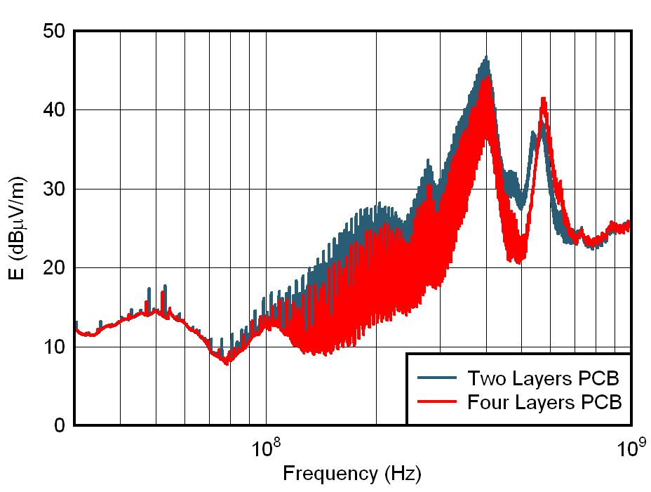
Board (left) and Four Layer Board (right)The effects of the four-layer board are highlighted in Figure 4-2. Overall, the transition to a four layer PCB improves the emission performance. The reduction in radiated field varies between 4 dB up to 10 dB for the most extreme cases.
 Figure 4-2 Radiated EMI Response of
Two-layer and Four-layer PCB