SLVAEP5A April 2020 – June 2021 LM3668 , TPS63000 , TPS63000-Q1 , TPS63001 , TPS63002 , TPS63010 , TPS63011 , TPS63020 , TPS63020-Q1 , TPS63021 , TPS63024 , TPS630241 , TPS630242 , TPS630250 , TPS630251 , TPS630252 , TPS63027 , TPS63030 , TPS63031 , TPS63036 , TPS63050 , TPS63051 , TPS63060 , TPS63061 , TPS63070 , TPS63802 , TPS63805 , TPS63806 , TPS63810 , TPS63811 , TPS63900 , TPS63901
2 EMI Sources
 Figure 2-1 EMI Sources in Non-inverting
Buck-boost Converter
Figure 2-1 EMI Sources in Non-inverting
Buck-boost ConverterFigure 2-1 highlights the main sources of EMI in a non-inverting buck-boost converter.
The first EMI source is the hot loop located between input capacitor (CIN) and SW2. The second loop responsible for EMI is the loop located between output capacitor (COUT) and SW3. The loops occurrence differs dependent on the converter operating mode. In Figure 2-1, the left loop exists during buck mode operation while the right most loop, during boost mode operation. Due to the switching logic, these loops will have high rates of change in current over time (di/dt). Taking into account the equivalent series inductance (ESL) of a capacitor and the equation of voltage over inductor Equation 1, it can be seen that these hot loops can give rise to unwanted voltages (vL).

The switching nodes L1 and L2 are another EMI source. Depending on the operation mode, L1 for buck and L2 for boost, these nodes experience high changes in voltage over time (dv/dt). A change in voltage can give rise to undesired currents in a capacitor as shown by Equation 2. Keeping in mind that capacitances can develop between inductor windings, the occurrence of parasitic currents (i2C) is possible.

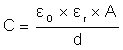
Besides the parasitic capacitance of the inductor, another capacitance also exists between the node and the ground layer. This capacitance is described by Equation 3 and it is strongly influenced by the distance (d) between the layer on which the node is located and the closest ground layer as well as by the area of the parallel plates (A). ε0 and εr are the permittivity of free space (ε0=8.85 pF/m) and the relative permittivity of the medium between the two plates.
The following sections will introduce tested solutions that reduce radiations. The proposed solutions are accompanied by measurements that prove their effectiveness. The measurements were conducted in accordance to the CISPR 16-2-3 standards and regulations referenced in Section 7.