SLVUC32B June 2021 – February 2022 DRA829J , DRA829J-Q1 , DRA829V , DRA829V-Q1 , TDA4VM , TDA4VM-Q1 , TPS6594-Q1
- Trademarks
- 1Introduction
- 2Device Versions
- 3Processor Connections
- 4Supporting Functional Safety Systems
-
5Static NVM Settings
- 5.1 Application-Based Configuration Settings
- 5.2 Device Identification Settings
- 5.3 BUCK Settings
- 5.4 LDO Settings
- 5.5 VCCA Settings
- 5.6 GPIO Settings
- 5.7 Finite State Machine (FSM) Settings
- 5.8 Interrupt Settings
- 5.9 POWERGOOD Settings
- 5.10 Miscellaneous Settings
- 5.11 Interface Settings
- 5.12 Multi-Device Settings
- 5.13 Watchdog Settings
- 6Pre-Configurable Finite State Machine (PFSM) Settings
- 7Impact of NVM Changes
- 8References
- 9Revision History
6.3.9 To Suspend-to-RAM (TO_S2R)
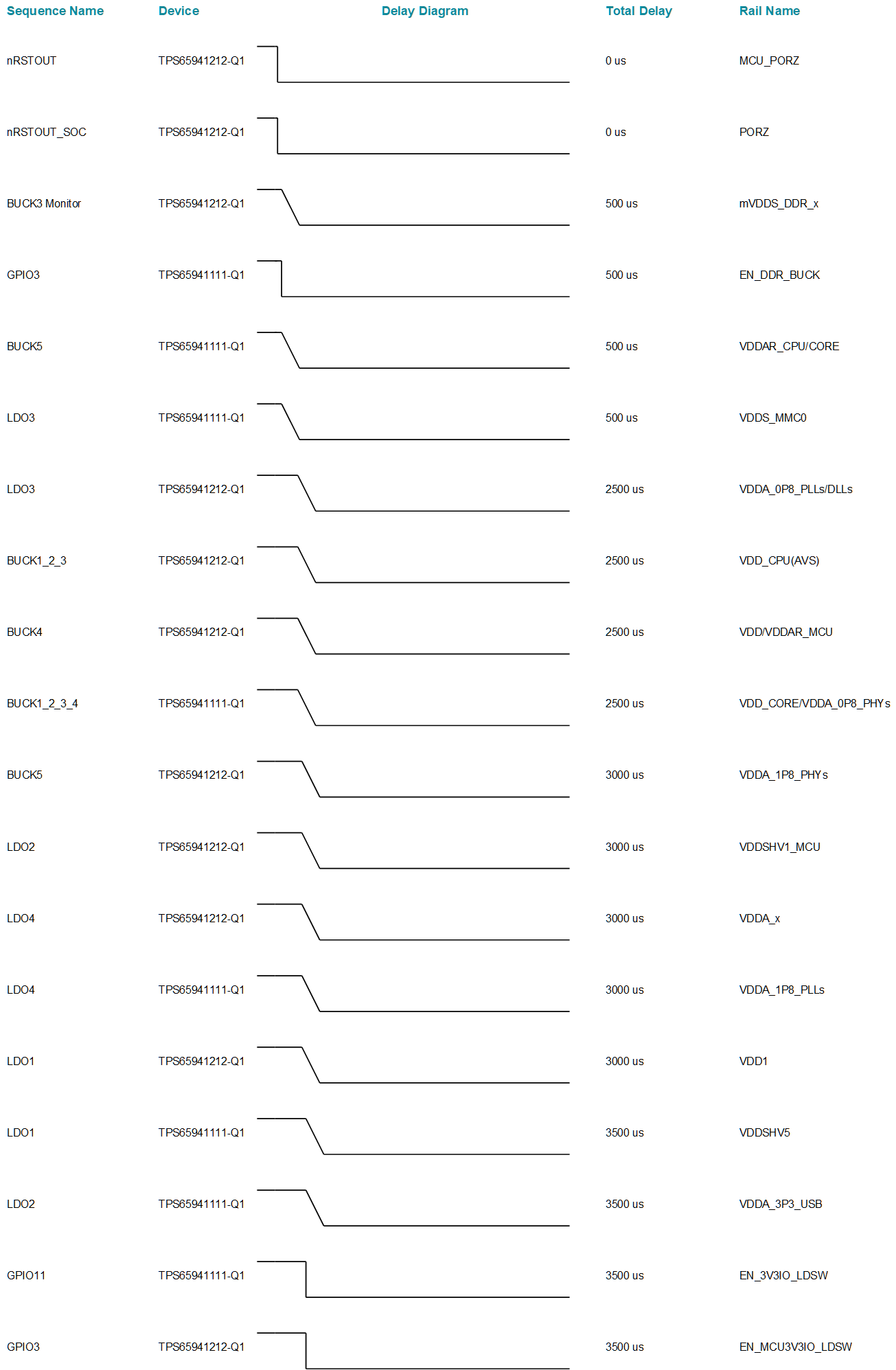
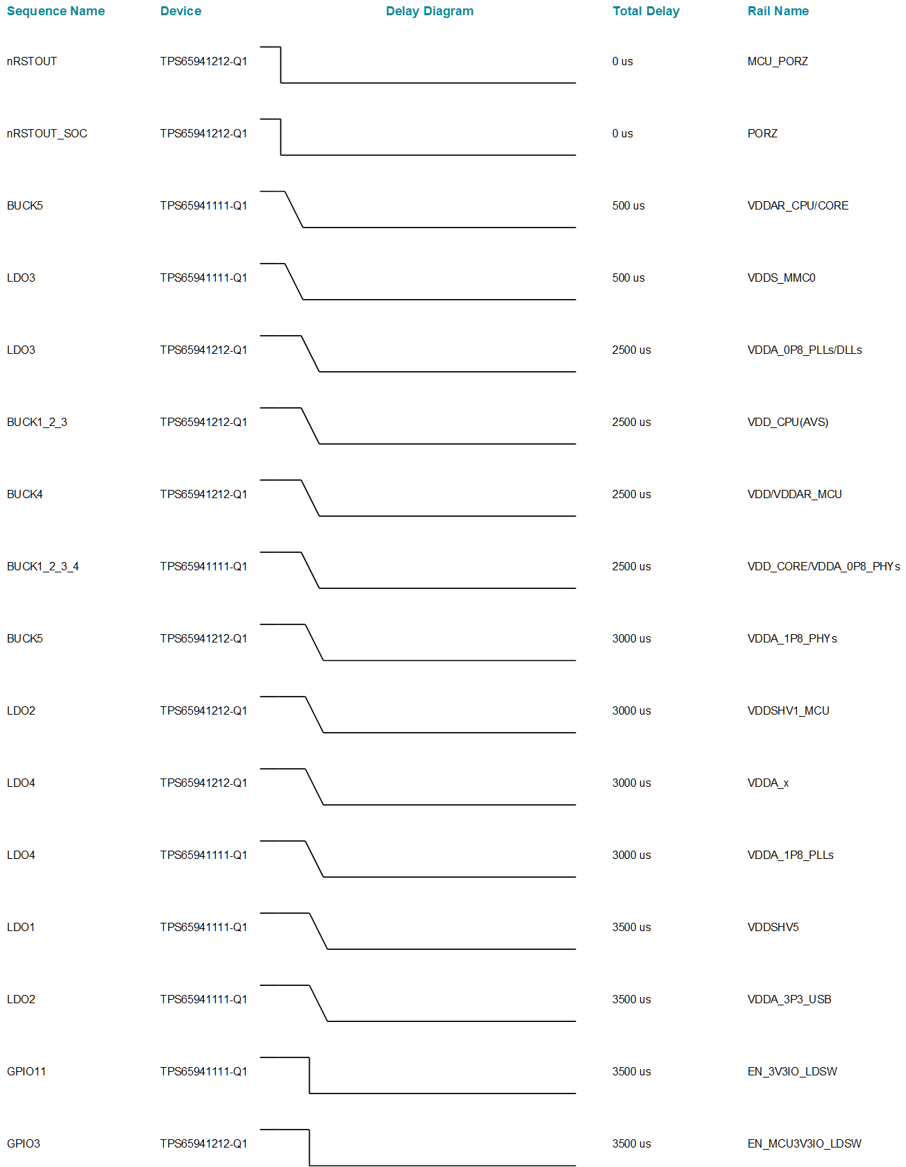
The C and D triggers, defined by the NSLEEPx bits or pins, trigger the S2R sequence. This sequence disables all power rails and GPIOs that are not supplying the retention rails, as described in Table 3-1. The sequence can be modified using the I2C_7 bit found in register FSM_I2C_TRIGGERS. These bits need to be set by I2C in both PMICs before a trigger for the retention state occurs. If the I2C_7 bit is set high in both PMICs, they enter the DDR retention state as shown in . The BUCK3 Monitor (mVDDS_DDR_x) as well as the LDO1 (VDD1) are not disabled and the GPIO3 of the TPS6591111 (EN_DDR_BUCK) is also unchanged. If I2C_7 is set low, these components associated with DDR do not remain active, as shown in Figure 6-12.
The following instructions are used to configure the PMICs at the beginning of the sequence:
// TPS65941212
// Set LPM_EN, Clear NRSTOUT_SOC and NRSTOUT
REG_WRITE_MASK_IMM ADDR=0x81 DATA=0x04 MASK=0xF8
// Set SPMI_LP_EN and FORCE_EN_DRV_LOW
REG_WRITE_MASK_IMM ADDR=0x82 DATA=0x18 MASK=0xE7
//TPS65941111
// Set SPMI_LP_EN
REG_WRITE_MASK_IMM ADDR=0x82 DATA=0x10 MASK=0xEF
Figure 6-12 TO_S2R and I2C_7 is Low on
Both PMICs
 Figure 6-13 To S2R and I2C_7 is High in
Both PMICs
Figure 6-13 To S2R and I2C_7 is High in
Both PMICsAt the end of the sequence, both PMICs set the LPM_EN and clear the CLKMON_EN and AMUXOUT_EN. The TPS65941212 device also performs an additional 16 ms delay based upon the contents of the register (PFSM_DELAY_REG_2) to ensure that the TPS65941212 sequence finishes last.