SLYY203B September 2021 – April 2023 BQ25125 , LM5123-Q1 , LMR43610 , LMR43610-Q1 , LMR43620 , LMR43620-Q1 , TPS22916 , TPS3840 , TPS62840 , TPS63900 , TPS7A02
- 1
- Overview
- At a glance
- Contributors to IQ
- Why low IQ creates new challenges
- How to break low IQ barriers
-
Electrical Characteristics
- 18
- Avoiding potential system pitfalls in a low-IQ designs
- Achieving low IQ, but not losing flexibility
- Reducing external component count to lower IQ in automotive applications automotive applications
- Smart on or enable features supporting low-IQ at the Smart on or enable features supporting low-IQ at the system level
- Conclusion
- Key product categories for low IQ
Transient response
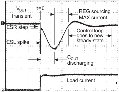
Power-supply accuracy is often limited by its transient response, which is characterized by its maximum voltage drop, settling time and voltage error integral (Figure 5).
 Figure 5 An output voltage
transient.
Figure 5 An output voltage
transient.The response time measures how fast a power device regulates back to the targeted output voltage after an abrupt change in load current or supply voltage. The response time comprises three stages: a delay time to react to the change, a recovery time from a dip or overshoot, and a settling time.
Low-IQ devices suffer from longer response times because the internal parasitic capacitors need to be charged to new operating points with relatively less current. The worst case is usually a step from no load to the maximum allowed load current. Such cases necessitate reactivating circuits that had been deactivated or reduced in power, causing an additional delay.
More importantly, the settling time itself suffers from reduced bias conditions. For a conventional differential input stage, the gain reduces linearly with the bias current, which causes a reduction in bandwidth and increased settling time.
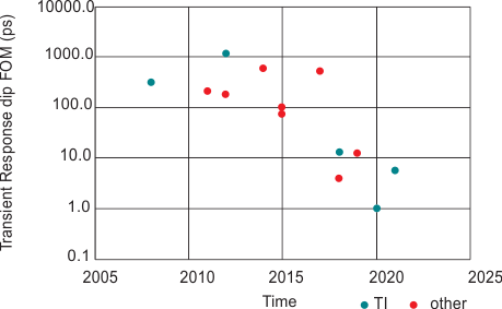
Calculating figures of merit (FOMs) helps the designer judge the overall performance of a power regulator. Equation 3 calculates a transient response dip FOM, normalizing the IQ by the maximum output current of the converter, the load current step (∆IO), the induced voltage drop (∆VO) and the output capacitor (CO). Figure 6 shows how FOM changes over time for a 5-V buck-boost converter. The smaller the FOM, the better the regulator’s performance.
 Figure 6 Transient response dip FOM
over time for a 5-V buck-boost converter.