SNVA856B May 2020 – October 2022 LM63615-Q1 , LM63625-Q1 , LM63635-Q1 , LMR33620 , LMR33620-Q1 , LMR33630 , LMR33630-Q1 , LMR33640 , LMR36006 , LMR36015 , TPS54360B , TPS54560B
- Working With Inverting Buck-Boost Converters
- Trademarks
- 1 Introduction
- 2 Inverting Buck-Boost Converter
- 3 Basic Operation
- 4 Operating Considerations of a Buck Based Inverting Buck-Boost
- 5 Component Selection for the IBB
- 6 General Considerations
- 7 Auxiliary Functions
- 8 Design Examples
- 9 Summary
- 10References
- 11Revision History
8.1 Converting +12 V to –5 V at 3 A
The design objectives are shown in Table 8-1 .
| VIN | VOUT | IOUT | SWITCHING FREQUENCY |
|---|---|---|---|
| +12 V | -5 V | 2.5 A | 400 kHz |
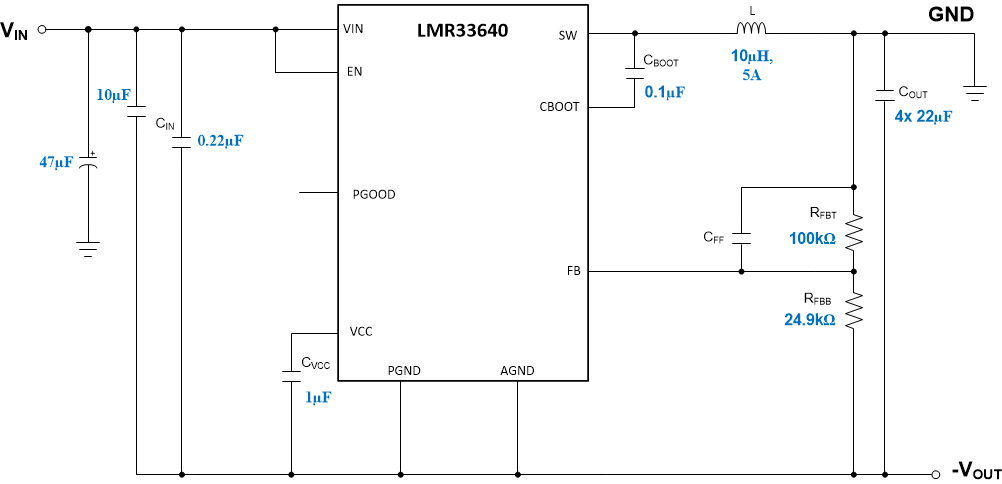
First, calculate the maximum voltage that the buck regulator will experience. This is simply the input voltage plus the output voltage; or +17 V. Next calculate the value of power inductance. For this example, use a ΔIL of 30% of IOUT or 0.75 A. We will also assume an efficiency of 0.85 throughout this example. Using Equation 8 we determine a value of 13 µH. We will choose a standard value of 10 µH. Rearranging Equation 8 we can calculate the actual value of ΔIL for the 10-µH inductor and use that for further calculations. With Equation 6 we find that IPEAK = 4.2 A and IVALLEY = 3.2 A. The average inductor current being 3.7 A. Looking at the LMR33640 we find that the minimum peak current limit is 4.8 A, and the minimum valley current limit is 3.9 A. These are within our limits, so we will use this device for the example. We would then choose a 10-µH inductor with at least a 5-A current rating. Note that in this example, you might be able to squeeze out 3 A of load current if the designer is OK with getting very close to the minimum guaranteed spec for the current limits. In this example, 3 A of load would give a typical peak current of about 4.9 A, and 3.9A for the valley current. Usually these values would be "too close for comfort", since the current will change with input voltage and the tolerance of the inductor. However, it may allow the designer to provide some head room for any momentary surge currents that may exist in the particular application.
For CIO we use the data sheet recommendations. We find that a 10-µF ceramic is required. In addition place a small case size 0.22-µF bypass cap close to the VIN and GND pins of the device. Also, as mentioned in the data sheet, CIN can be a small aluminum electrolytic of 47 µF to 100 µF. The data sheet recommends 4 × 22-µF ceramics for the output capacitor bank for a 5-V, 4-A, 400-kHz design. This is a good starting point for our IBB. Allow space on the PCB for extra output capacitors if they are required to improve the load transient response and/or the loop stability. The values of CBOOT and CVCC remain the same as with the positive buck; 0.1 µF and 1 µF, respectively.
The LMR33640 requires a feedback voltage divider. Use the data sheet values for a 5-V output. In this case we use RFBT = 100 kΩ and RFBB = 24.9 kΩ. Also, leave a place on the PCB for a CFF capacitor so that the loop stability can be optimized. Choose the LMR33640A to get 400 kHz. If the enable or PGOOD functions are needed, one of the level shifters shown previously can be used.
Once the design is completed, measure the efficiency to ensure that the converter can supply the required load current over the entire range of input voltage and ambient temperature. The complete schematic for the +12 V to –5 V design using the LMR33640 is shown in Figure 8-1.
 Figure 8-1 +12 V to –5 V, 3-A Design with the LMR33640