SPRAA99C March   2008  – May 2021 AM3351 , AM3352 , AM3354 , AM3356 , AM3357 , AM3358 , AM3359 , AM4372 , AM4376 , AM4377 , AM4378 , AM4379 , OMAPL138B-EP , TMUX646


  1.   Trademarks
  2. 1Introduction
  3. 2PCB Design Considerations
    1. 2.1 Solder Land Areas
    2. 2.2 Conductor Width/Spacing
    3. 2.3 High-Density Routing Techniques
    4. 2.4 Via Density
    5. 2.5 Conventional PCB Design
    6. 2.6 Advanced Design Methods
  4. 3Reliability
    1. 3.1 Reliability Calculations
    2. 3.2 Package Characteristics
    3. 3.3 Thermal Modeling
  5. 4Surface-Mounting nFBGA Packages
    1. 4.1 Design for Manufacturability (DFM)
    2. 4.2 Solder Paste
    3. 4.3 Solder Ball Collapse
    4. 4.4 Reflow
    5. 4.5 Inspection
  6. 5Packing and Shipping
    1. 5.1 Tray Packing Method
    2. 5.2 Tape-and-Reel Packing Method
    3. 5.3 Tape Format
    4. 5.4 Device Insertion
    5. 5.5 Packaging Method
  7. 6Sockets
    1. 6.1 The Design Challenge
    2. 6.2 Contacting the Ball
    3. 6.3 Pinch Contact
    4. 6.4 Micro Tuning Fork Contact
    5. 6.5 Texas Instruments Sockets
  8. 7Summary
  9.   A Frequently Asked Questions
    1.     A.1 Package Questions
    2.     A.2 Assembly Questions
    3.     A.3 Small Body nFBGA Package Questions
  10.   B Package Data Sheets
  11.   C Thermal Modeling Results
  12.   Revision History

Conductor Width/Spacing

Figure 2-4 presents some design considerations based on commonly used PCB design rules. Conventionally, the pads are connected by wide copper traces to other devices or to plated through holes (PTH). As a rule, the mounting pads must be isolated from the PTH. Placing the PTH interstitially to the land pads often achieves this.
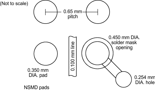
GUID-C05863C9-5D3D-43F4-9884-0AB49DC9A7A6-low.gif Figure 2-4 PCB Design Considerations (Conventional)