SPRAC94D September 2018 – March 2022 AFE030 , AFE031 , TMS320F28075 , TMS320F28075-Q1 , TMS320F28076 , TMS320F28374D , TMS320F28374S , TMS320F28375D , TMS320F28375S , TMS320F28375S-Q1 , TMS320F28376D , TMS320F28376S , TMS320F28377D , TMS320F28377D-EP , TMS320F28377D-Q1 , TMS320F28377S , TMS320F28377S-Q1 , TMS320F28379D , TMS320F28379D-Q1 , TMS320F28379S
- Trademarks
- 1 FSK Overview
- 2 Hardware Overview
- 3 Interfacing With the AFE03x
- 4 Transmit Path
- 5 Receive Path
- 6 Interfacing With a Power Line
- 7 Summary
- 8 References
- 9 Schematics
- 10Revision History
6.2.2 The Ratio of the Transformer
Most power-line communication transformers are compact, with turns ratios between 1:1 and 4:1, low leakage inductance, and approximately 1-mH of winding inductance. This inductance in series with the high-voltage capacitor results in a voltage divider attenuating the ac mains voltage down to negligible levels at the module output.
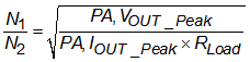
To determine the optimal turns ratio for the transformer it must be based on the PA's capabilities of maximum output swing and maximum output current to achieve maximum power transfer into the load.
There are three cases where a one limitation is dominant than the others.
- Case 1:
If the turns ratio of the transformer is greater than the ideal calculated value, the TX output of the AFE031 is limited by the voltage swing of the PA.
- Case 2:
If the turns ratio of the transformer is less than the ideal calculated value, the TX output of the AFE031 is limited by the maximum output current from the PA.
- Case 3:
If the turns ratio of the transformer is equal to the ideal calculated value, the TX maximum output occurs as the amplifier approaches both its maximum output voltage and maximum output current resulting in maximum power transfer to the load.
It is also important to be aware that the transformer affects the coupling emission performance of the EN50065-1 when under a 2-MHz frequency. In order to compensate, TI recommends using products from Wurth Electronik.