SPRAC94D September   2018  – March 2022 AFE030 , AFE031 , TMS320F28075 , TMS320F28075-Q1 , TMS320F28076 , TMS320F28374D , TMS320F28374S , TMS320F28375D , TMS320F28375S , TMS320F28375S-Q1 , TMS320F28376D , TMS320F28376S , TMS320F28377D , TMS320F28377D-EP , TMS320F28377D-Q1 , TMS320F28377S , TMS320F28377S-Q1 , TMS320F28379D , TMS320F28379D-Q1 , TMS320F28379S


  1.   Trademarks
  2. FSK Overview
  3. Hardware Overview
    1. 2.1 Block Diagram
    2. 2.2 Hardware Setup
  4. Interfacing With the AFE03x
    1. 3.1 Configuring the AFE031
  5. Transmit Path
    1. 4.1 FSK Example Specifications
    2. 4.2 PWM Mode
      1. 4.2.1 Software Implementation
      2. 4.2.2 Testing Results
      3. 4.2.3 HRPWM vs. EPWM
    3. 4.3 DAC Mode
      1. 4.3.1 Software Implementation
      2. 4.3.2 Testing Results
      3. 4.3.3 OFDM Ability
    4. 4.4 Porting TX to LAUNCHXL-F280049C
      1. 4.4.1 PWM Mode Specific Porting
      2. 4.4.2 DAC Mode Specific Porting
  6. Receive Path
    1. 5.1 Receive Path Overview
    2. 5.2 Receiver Software Implementation
      1. 5.2.1 Initial Setup and Parameters
      2. 5.2.2 Interrupt Service Routines
      3. 5.2.3 Run Time Operation
      4. 5.2.4 Testing Results
      5. 5.2.5 System Utilization
      6. 5.2.6 Device Dependency and Porting
    3. 5.3 Tuning and Calibration
      1. 5.3.1 Setting the AFE03X's PGAs
      2. 5.3.2 Automatic Gain Control (AGC)
      3. 5.3.3 Setting the Bit Detection Threshold
      4. 5.3.4 FSK Correlation Detector Library
    4. 5.4 Porting RX to LAUNCHXL-F280049C
  7. Interfacing With a Power Line
    1. 6.1 Line Coupling
    2. 6.2 Coupling to an AC Line
      1. 6.2.1 Low Voltage Capacitor
      2. 6.2.2 The Ratio of the Transformer
      3. 6.2.3 HV Capacitor
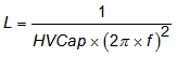
      4. 6.2.4 HV Side Inductor
    3. 6.3 Coupling to DC Line
    4. 6.4 Protection Circuit
      1. 6.4.1 Metal Oxide Varistors
      2. 6.4.2 Transient Voltage Suppressors
      3. 6.4.3 Current Steering Diodes
    5. 6.5 Determining PA Power Supply Requirements
  8. Summary
  9. References
  10. Schematics
    1. 9.1 Schematics (PWM Mode)
    2. 9.2 Schematics (DAC Mode)
  11. 10Revision History

HV Side Inductor

The inductor that is connected in series with the HV capacitor is required when driving low line impedances and the HV Cap is restricted to approximately 470 nF, for the reasons previously stated. In applications that operate in the Cenelec A band, the impedance of the 470-nF capacitance at 40 kHz is approximately 8.5 Ω. If the application requires the ability to drive a 2-Ω load, for example, this series impedance is restrictive. Adding the series inductor can mitigate this effect. To properly select the value of the inductance, the operating frequency range of the system must be known. A common example would be the PRIME frequency band, which is approximately 40 kHz to 90 kHz. Selecting the HV Cap and inductor to have a resonant frequency in the center of the frequency band is recommended, and results in a series inductor value of 12.8 µH and HV Cap value of 470 nF.

Equation 5. GUID-5AED7D56-F0DC-40AB-B9EC-113736CBE3E7-low.gif

The inductor should be sized to be capable of withstanding the maximum load current without saturation.