SPRAC94D September 2018 – March 2022 AFE030 , AFE031 , TMS320F28075 , TMS320F28075-Q1 , TMS320F28076 , TMS320F28374D , TMS320F28374S , TMS320F28375D , TMS320F28375S , TMS320F28375S-Q1 , TMS320F28376D , TMS320F28376S , TMS320F28377D , TMS320F28377D-EP , TMS320F28377D-Q1 , TMS320F28377S , TMS320F28377S-Q1 , TMS320F28379D , TMS320F28379D-Q1 , TMS320F28379S
- Trademarks
- 1 FSK Overview
- 2 Hardware Overview
- 3 Interfacing With the AFE03x
- 4 Transmit Path
- 5 Receive Path
- 6 Interfacing With a Power Line
- 7 Summary
- 8 References
- 9 Schematics
- 10Revision History
1 FSK Overview
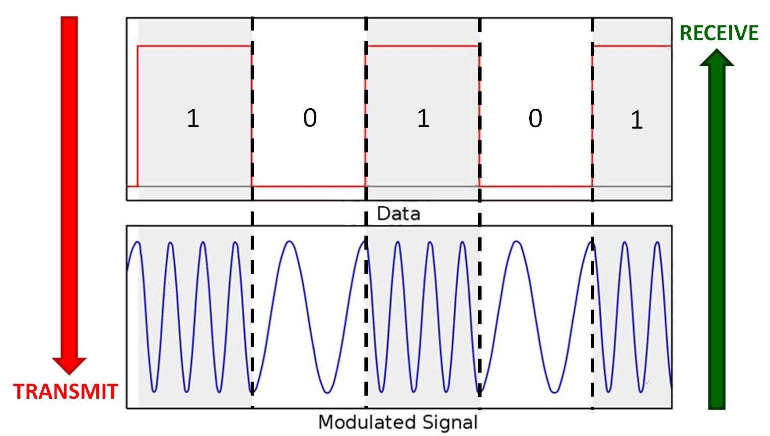
Frequency Shift Keying (FSK) is a modulation scheme that utilizes discrete changes of frequency to transmit and receive digital data. One of the simplest subsections of this modulation scheme, and also the modulation used in this demo, is called Binary Frequency Shift Keying (BFSK).
In this scheme, the system is switching between two discrete frequencies: the Mark Frequency (“1”) and the Space Frequency (“0”). These frequencies correlate directly to the bit value of the transmitted data.
Figure 1-1 shows what this looks like in the time domain.
 Figure 1-1 Binary FSK in the Time
Domain
Figure 1-1 Binary FSK in the Time
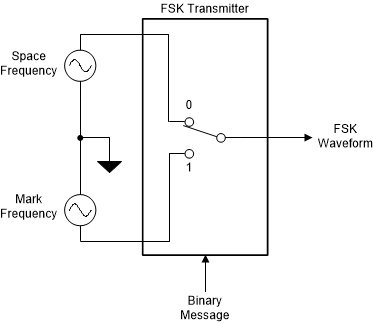
DomainFigure 1-2 shows an example of a simplified FSK transmitter where the block consists of two oscillators with an internal clock as well as an input binary sequence to control the position of the switch.
 Figure 1-2 Transmitter Example
The two oscillators, producing a higher (space) and a lower (mark) frequency signals, are connected to a switch along with an internal clock. A clock is applied internally to both oscillators to avoid phase discontinuities of the output waveform during the transmission of the message. The binary input sequence is applied to choose the frequencies according to the binary input. In this case, binary "0" corresponds to the output of the space frequency and binary "1" corresponds to the output of the mark frequency.
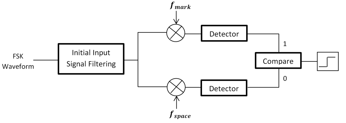
Figure 1-3 shows an example of a simplified FSK receiver to convert a received signal back into the desired digital information.
 Figure 1-3 Receiver Example
A FSK waveform is initially filtered and then mixed with signals of the desired mark (fmark ) and space (fspace ) frequencies. The output is run through a detector algorithm and the results are compared to decipher if the signal being received pertains to a mark, binary "1", or space, binary"0". Additional functionality is included to decipher received bits, based on the duration of the received mark or space signal, and handle the boundaries between consecutive bits.
This is a simple overview on how FSK works. The following sections discuss how this is implemented on a C2000 device.