SPRAC94D September 2018 – March 2022 AFE030 , AFE031 , TMS320F28075 , TMS320F28075-Q1 , TMS320F28076 , TMS320F28374D , TMS320F28374S , TMS320F28375D , TMS320F28375S , TMS320F28375S-Q1 , TMS320F28376D , TMS320F28376S , TMS320F28377D , TMS320F28377D-EP , TMS320F28377D-Q1 , TMS320F28377S , TMS320F28377S-Q1 , TMS320F28379D , TMS320F28379D-Q1 , TMS320F28379S
- Trademarks
- 1 FSK Overview
- 2 Hardware Overview
- 3 Interfacing With the AFE03x
- 4 Transmit Path
- 5 Receive Path
- 6 Interfacing With a Power Line
- 7 Summary
- 8 References
- 9 Schematics
- 10Revision History
6.4.2 Transient Voltage Suppressors
A TVS is a very fast-acting clamping device that turns on in the case of an overvoltage condition, shunting the surge of current into ground. TVSs are rated primarily by the power handling capability and the clamping voltage. TVSs are available in either unidirectional or bi-directional configurations.
 Figure 6-8 Bi-Directional TVS Diode
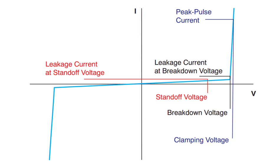
For power-line communication applications, a bi-directional TVS is recommended; the component is placed next to the line coupling transformer. Figure 6-9 shows the I/V characteristics for a typical bi-directional TVS.
 Figure 6-9 Typical Bi-Directional TVS I/V Characteristics
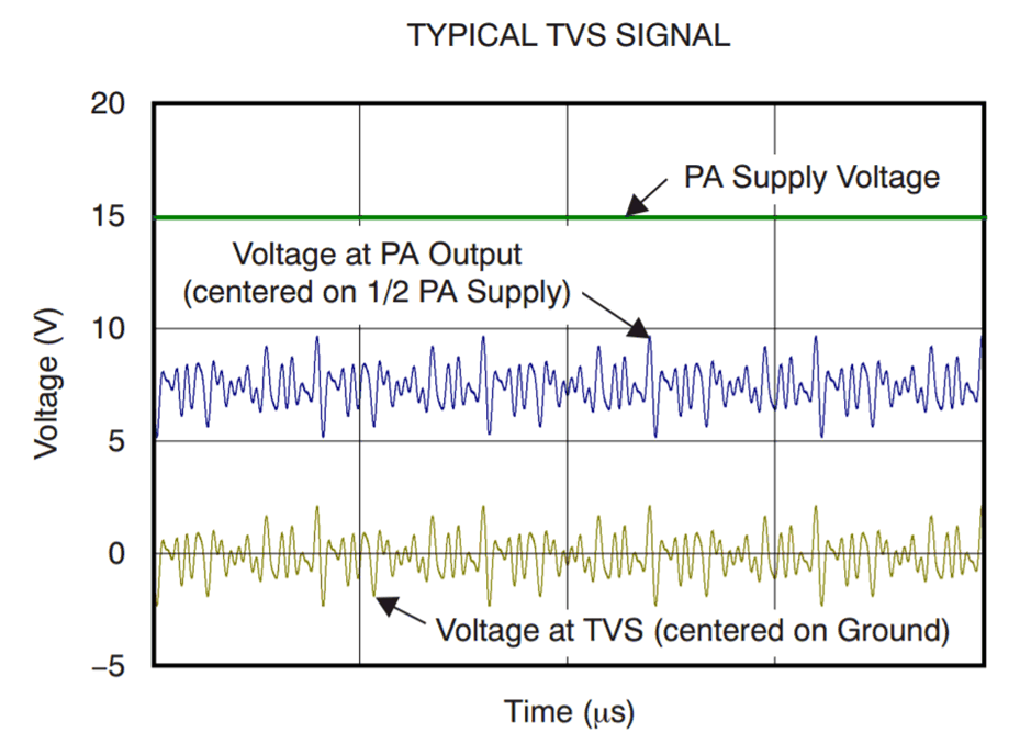
As a surge or pulse on the ac line occurs, the voltage rises across the TVS. If the voltage rises higher than the TVS breakdown voltage, the TVS turns on and rapidly changes from high impedance to low impedance, shunting current into ground. Note that the low-voltage capacitor between the PA output and the TVS blocks any dc voltage at the TVS. As a result, the normal FSK or OFDM signal from the PA appears to be centered around ground at the TVS. This condition requires the TVS to be bi-directional.
Figure 6-10 illustrates this concept.
 Figure 6-10 Typical Signal at the TVS
Because the signal is symmetric around ground at the TVS, the TVS breakdown voltage should be equal to approximately one-half of the PA power-supply voltage. It is important for the TVS to remain off during normal operation to avoid clipping and introducing distortions to the output signal. It is also important that the TVS turn on and clamp at the lowest possible voltage beyond normal operation to provide maximum protection.
This BoosterPack was designed with surge protection parts. A bi-directional transient-voltage suppression (TVS) diode with a shunt connection to attach on the LV side of the transformer is used to clamp the voltage of a surge. The stable voltage of the TVS must be exactly 1/2 of the PA supply voltage of the AFE, meaning a 15-V AFE must use a 7.5-V TVS. This 1/2 ratio is based on the fact that:
- The PA of the AFE is a type AB, which uses a single power rail. So, the 12-V powered PA TX output is at a 6-V bias with a ±6-V amplitude, meaning that the signal has a ±6-V range. While on transmission, the TVS must not be allowed to saturate the signal, so the stable voltage must be kept to ≥ ½ of the PA power rail.
- If a 12-V PA uses a 7.5-V TVS, during the arrival of a surge pulse, the LV side bias is locked-on at 7.5 V, but if the surge occurs at the exact moment of a TX maximum amplitude (which is 6 V), then the signal on the TX route is 7.5 V + 6 V = 13.5 V, which is higher than the power rail and causes damage to the PA of the AFE. So, the TVS voltage must be ≤ 1/2 of the PA power rail.