SPRAD61A March 2023 – November 2023 AM2732 , AM2732 , AM2732-Q1 , AM2732-Q1
- 1
- Abstract
- Trademarks
- 1 Introduction
- 2 Power
- 3 Clocking
- 4 Resets
- 5 Bootstrapping
- 6 JTAG Emulators and Trace
- 7 Multiplexed Peripherals
- 8 Digital Peripherals
- 9 Layer Stackup
- 10Vias
- 11BGA Power Fan-Out and Decoupling Placement
- 12References
- 13Revision History
1 Introduction
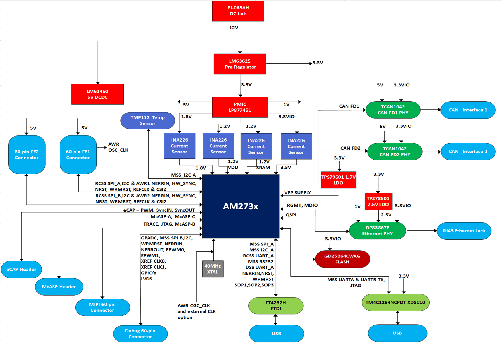
The AM273x family of microcontrollers is a highly-integrated, high performance microcontroller based on the Arm Cortex-R5F and a C66x floating-point DSP cores. The device enables Original-Equipment Manufacturers (OEM) and Original-Design Manufacturers (ODM) to quickly bring to market devices with robust software support, rich user interfaces, and high performance, through the maximum flexibility of a fully integrated, mixed processor solution. A typical AM273x based design is shown in Figure 1-1. This diagram is excerpted from the AM273x EVM (TMDS273GPEVM) system block diagram. As can be seen below the AM273x devices offer designers a wide range of digital connectivity, audio, radar and analog sensor feedback options.
 Figure 1-1 Typical AM273x System
Block Diagram (Based on TMDS273GPEVM Design)
Figure 1-1 Typical AM273x System
Block Diagram (Based on TMDS273GPEVM Design)To quickly achieve a working system with the numerous cores peripherals and pin multiplexing options available on the AM273x MCU, this document should be referenced along with the other key AM273x collateral references. These include:
- The AM273x Sitara™ Microcontroller Data Sheet [1] is the primary resource for all device pinout and pin-level multiplexing options.
- The SYSCONFIG [4] pinmux planning tool should be utilized when starting a new AM273x pinout and driver utilization.
- The AM273x Sitara™ Microcontroller Technical Reference Manual [2] documents detail each core and peripheral subsystem from a conceptual, usage and programming model perspective.
- The AM273x MCU-SDK [7] ties the data sheet and technical reference manual together with software system and peripheral usage examples.