SPRAD61A March 2023 – November 2023 AM2732 , AM2732 , AM2732-Q1 , AM2732-Q1
- 1
- Abstract
- Trademarks
- 1 Introduction
- 2 Power
- 3 Clocking
- 4 Resets
- 5 Bootstrapping
- 6 JTAG Emulators and Trace
- 7 Multiplexed Peripherals
- 8 Digital Peripherals
- 9 Layer Stackup
- 10Vias
- 11BGA Power Fan-Out and Decoupling Placement
- 12References
- 13Revision History
2.3 Power Decoupling and Filtering
Table 2-1 describes the initial BGA decoupling and power filtering required for the AM273x. These were based on the initial simulation feedback of the AM273 GPEVM PCB and AM273x package with the above transient use-cases.
The decoupling network presented in the below sections and in the AM273x EVM schematics and layouts are reasonable starting points for any AM273x PCB design. Additional placement guidance for the decoupling network is provided in Section 11. However, due to specific PCB routing differences and the resulting plane capacitance and decoupling mounting inductances and other parasitics, it is highly recommended that designers simulate and measure their specific power distribution network performance. Simulations and measurements should ideally be done with target application software active and intended operating environment conditions applied to the system.
| Device Supply | Quantity | Comment | Part Number | Manufacturer |
|---|---|---|---|---|
| 1.2-V VDD_CORE | 2 | 2.2 µF, 6.3 V, ± 10%, X7R, AEC-Q200 Grade 1, 0603 | GCM188R70J225KE22D | Murata |
| 5 | 0.22 µF, 16 V,± 10%, X7R, AEC-Q200 Grade 1, 0402 | GCM155R71C224KE02D | Murata | |
| 3 | 0.01 µF, 50 V, ± 10%, X7R, AEC-Q200 Grade 1, 0402 | CGA2B3X7R1H103K050BB | TDK | |
| 1.2-V SRAM | 1 | 0.22 µF, 16 V, ± 10%, X7R, AEC-Q200 Grade 1, 0402 | GCM155R71C224KE02D | Murata |
| 2 | 0.1 µF, 16 V, ± 10%, X7R, 0402 | GCM155R71C104KA55D | Murata | |
| 1.8-V IO Supply | 4 | 0.22 µF, 16 V, ± 10%, X7R, AEC-Q200 Grade 1, 0402 | GCM155R71C224KE02D | Murata |
| 3.3-V IO Supply | 1 | 2.2 µF, 6.3 V, ± 10%, X7R, AEC-Q200 Grade 1, 0603 | GCM188R70J225KE22D | Murata |
| 6 | 0.22 µF, 16 V, ± 10%, X7R, AEC-Q200 Grade 1, 0402 | GCM155R71C224KE02D | Murata | |
| 1.8-V ADC Supply | 1 | 0.22 µF, 16 V, ± 10%, X7R, AEC-Q200 Grade 1, 0402 | GCM155R71C224KE02D | Murata |
| 1.8-V Clock Supply | 1 | 0.22 µF, 16 V, ± 10%, X7R, AEC-Q200 Grade 1, 0402 | GCM155R71C224KE02D | Murata |
| 1.8-V CSI Supply | 1 | 0.22 µF, 16 V, ± 10%, X7R, AEC-Q200 Grade 1, 0402 | GCM155R71C224KE02D | Murata |
| 1.8-V LVDS Supply | 1 | 0.22 µF, 16 V, ± 10%, X7R, AEC-Q200 Grade 1, 0402 | GCM155R71C224KE02D | Murata |
| VNWA Supply | 1 | 0.1 µF, 16 V, ± 10%, X7R, 0402 | GCM155R71C104KA55D | Murata |
| Bandgap Supply | 1 | 0.047 µF, 50 V, ± 10%, X7R, AEC-Q200 Grade 1, 0402 | CGA2B3X7R1H473K050BB | TDK |
| VPP Supply | 1 | 0.1 µF, 16 V, ± 10%, X7R, 0402 | GCM155R71C104KA55D | Murata |
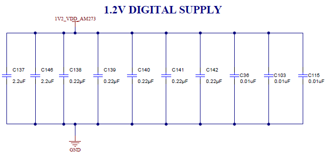 Figure 2-4 AM273x GPEVM Excerpt – 1.2 V
Power Decoupling Schematic
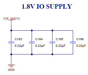 Figure 2-5 AM273x GPEVM Excerpt – 1.8 V
Digital I/O Decoupling Schematic
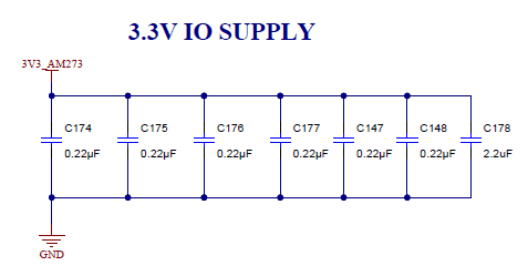 Figure 2-6 AM273x GPEVM Excerpt – 3.3 V
Digital I/O Decoupling Schemati
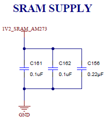 Figure 2-7 AM273x GPEVM Excerpt – SRAM
Decoupling Schematic
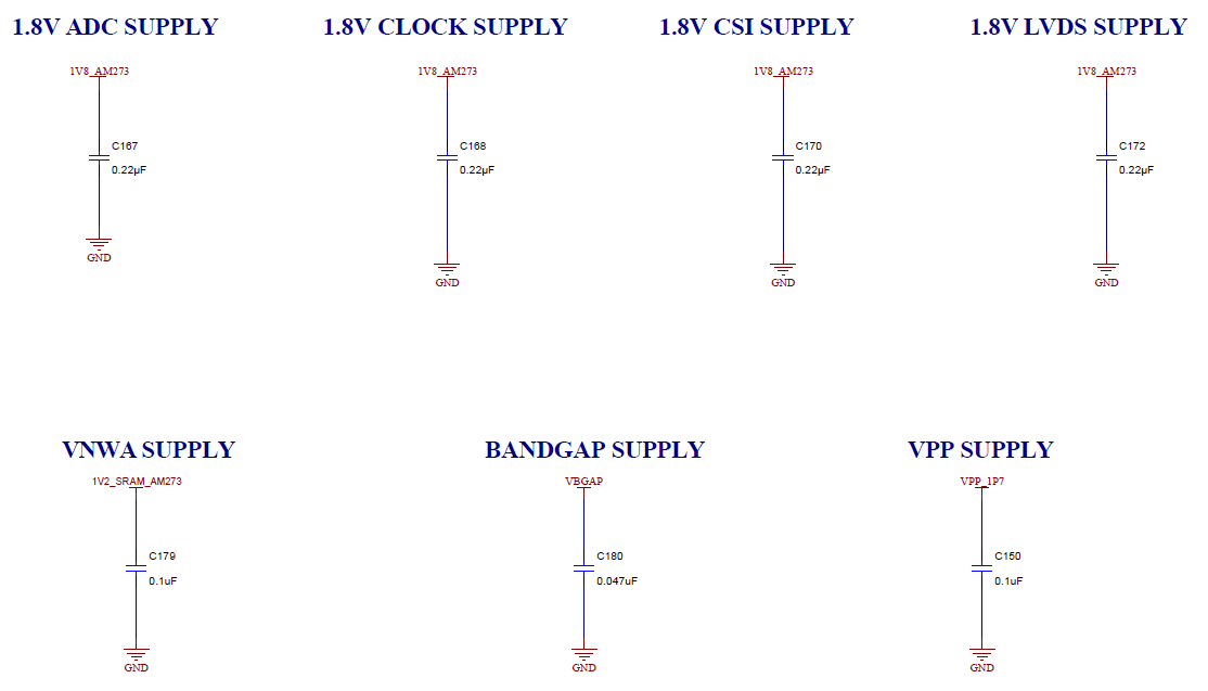 Figure 2-8 AM273x GPEVM Excerpt –
Additional Decoupling Schematic