SPRAD61A March   2023  – November 2023 AM2732 , AM2732 , AM2732-Q1 , AM2732-Q1


  1.   1
  2.   Abstract
  3.   Trademarks
  4. Introduction
    1. 1.1 Acronyms
  5. Power
    1. 2.1 Discrete DC-DC Power Solution
    2. 2.2 Integrated PMIC Power Solution
    3. 2.3 Power Decoupling and Filtering
    4. 2.4 Power Consumption
  6. Clocking
    1. 3.1 Crystal and Oscillator Input Options
    2. 3.2 Output Clock Generation
    3. 3.3 Crystal Selection and Shunt Capacitance
    4. 3.4 Crystal Placement and Routing
  7. Resets
  8. Bootstrapping
    1. 5.1 SOP Signal Implementation
    2. 5.2 QSPI Memory Controller Implementation
    3. 5.3 ROM QSPI Boot Requirements
  9. JTAG Emulators and Trace
  10. Multiplexed Peripherals
  11. Digital Peripherals
    1. 8.1 General Digital Peripheral Routing Guidelines
  12. Layer Stackup
    1. 9.1 TMDS273GPEVM Layer Stackup
      1. 9.1.1 TMDS273GPEVM Key Stackup Features
    2. 9.2 Four Layer ZCE Example Layer Stackup
      1. 9.2.1 ZCE Four Layer Example Key Stackup Features
    3. 9.3 Four Layer NZN Example Layer Stackup
      1. 9.3.1 NZN Four Layer Example Key Stackup Features
  13. 10Vias
  14. 11BGA Power Fan-Out and Decoupling Placement
    1. 11.1 Ground Return
      1. 11.1.1 Ground Return - TMDS273GPEVM
      2. 11.1.2 Ground Return - ZCE Four Layer Example
      3. 11.1.3 Ground Return - NZN Four Layer Example
    2. 11.2 1.2 V Core Digital Power
      1. 11.2.1 1.2 V Core Digital Power Key Layout Considerations
        1. 11.2.1.1 1.2V Core Layout - TMDS273GPEVM
        2. 11.2.1.2 1.2V Core Layout - ZCE Four Layer Example
        3. 11.2.1.3 1.2V Core Layout - NZN Four Layer Example
    3. 11.3 3.3 V Digital and Analog Power
      1. 11.3.1 3.3 V Digital and Analog Power Key Layout Considerations
        1. 11.3.1.1 3.3V Digital and Analog Layout - TMDS273GPEVM
        2. 11.3.1.2 3.3V Digital and Analog Layout - ZCE Four Layer Example
        3. 11.3.1.3 3.3V Digital and Analog Layout - NZN Four Layer Example
    4. 11.4 1.8 V Digital and Analog Power
      1. 11.4.1 1.8 V Digital and Analog Power Key Layout Considerations
        1. 11.4.1.1 1.8V Digital and Analog Layout - TMDS273GPEVM
        2. 11.4.1.2 1.8V Digital and Analog Layout - ZCE Four Layer Example
        3. 11.4.1.3 1.8V Digital and Analog Layout - NZN Four Layer Example
  15. 12References
  16. 13Revision History

JTAG Emulators and Trace

The AM273x MCU supports multiple different classes of JTAG emulators with or without additional ARM Trace capture capabilities.

For out of box convenience the TMDS273GPEVM implements an onboard XDS110 emulator with JTAG and auxiliary UART-USB bridge using a TI TM4C MCU. However, for actual custom systems, a simpler JTAG/Trace debug header should be implemented. This allows for external JTAG and Trace pods to be attached to the system as needed during development. The header can then be removed entirely or depopulated for full production of the system to save cost.

One popular JTAG and Trace implementation is the MIPI industry standard MIPI-60 shown in [5]. This is based on the Samtec QSH-030-01-L-D-A. This implementation is compatible with TI XDS560v2 JTAG/Trace pods as well as other third-party JTAG/Trace pods. Additional TI JTAG debugger connections can be found in [6].
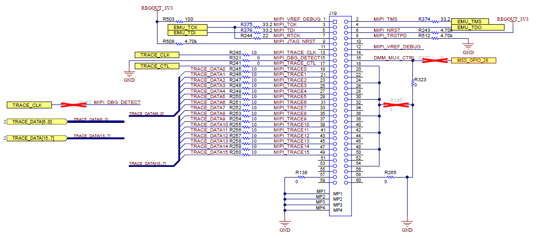
GUID-A888DF5E-9E86-4049-B321-A5982FE973FF-low.png Figure 6-1 Example MIPI-60 JTAG and 16-Bit Trace Implementation

Additional, non-TI JTAG debug and Trace systems are still being tested. Further guidance is planned in future revisions of this document.