SPRAD61A March   2023  – November 2023 AM2732 , AM2732 , AM2732-Q1 , AM2732-Q1


  1.   1
  2.   Abstract
  3.   Trademarks
  4. Introduction
    1. 1.1 Acronyms
  5. Power
    1. 2.1 Discrete DC-DC Power Solution
    2. 2.2 Integrated PMIC Power Solution
    3. 2.3 Power Decoupling and Filtering
    4. 2.4 Power Consumption
  6. Clocking
    1. 3.1 Crystal and Oscillator Input Options
    2. 3.2 Output Clock Generation
    3. 3.3 Crystal Selection and Shunt Capacitance
    4. 3.4 Crystal Placement and Routing
  7. Resets
  8. Bootstrapping
    1. 5.1 SOP Signal Implementation
    2. 5.2 QSPI Memory Controller Implementation
    3. 5.3 ROM QSPI Boot Requirements
  9. JTAG Emulators and Trace
  10. Multiplexed Peripherals
  11. Digital Peripherals
    1. 8.1 General Digital Peripheral Routing Guidelines
  12. Layer Stackup
    1. 9.1 TMDS273GPEVM Layer Stackup
      1. 9.1.1 TMDS273GPEVM Key Stackup Features
    2. 9.2 Four Layer ZCE Example Layer Stackup
      1. 9.2.1 ZCE Four Layer Example Key Stackup Features
    3. 9.3 Four Layer NZN Example Layer Stackup
      1. 9.3.1 NZN Four Layer Example Key Stackup Features
  13. 10Vias
  14. 11BGA Power Fan-Out and Decoupling Placement
    1. 11.1 Ground Return
      1. 11.1.1 Ground Return - TMDS273GPEVM
      2. 11.1.2 Ground Return - ZCE Four Layer Example
      3. 11.1.3 Ground Return - NZN Four Layer Example
    2. 11.2 1.2 V Core Digital Power
      1. 11.2.1 1.2 V Core Digital Power Key Layout Considerations
        1. 11.2.1.1 1.2V Core Layout - TMDS273GPEVM
        2. 11.2.1.2 1.2V Core Layout - ZCE Four Layer Example
        3. 11.2.1.3 1.2V Core Layout - NZN Four Layer Example
    3. 11.3 3.3 V Digital and Analog Power
      1. 11.3.1 3.3 V Digital and Analog Power Key Layout Considerations
        1. 11.3.1.1 3.3V Digital and Analog Layout - TMDS273GPEVM
        2. 11.3.1.2 3.3V Digital and Analog Layout - ZCE Four Layer Example
        3. 11.3.1.3 3.3V Digital and Analog Layout - NZN Four Layer Example
    4. 11.4 1.8 V Digital and Analog Power
      1. 11.4.1 1.8 V Digital and Analog Power Key Layout Considerations
        1. 11.4.1.1 1.8V Digital and Analog Layout - TMDS273GPEVM
        2. 11.4.1.2 1.8V Digital and Analog Layout - ZCE Four Layer Example
        3. 11.4.1.3 1.8V Digital and Analog Layout - NZN Four Layer Example
  15. 12References
  16. 13Revision History

3.3V Digital and Analog Layout - TMDS273GPEVM

A common step-down-converter generates a 3.3 V rail that is supplied to the PMIC on the AM273x GPEVM as well as the peripheral 3.3 V system needs and LDOs for the 2.5 V Ethernet and 1.7V VPP power rails. The PMIC generates a 3.3 V rail on the VIO_LDO output, which supplies the 3.3 V analog and digital supplies for all of the AM273x digital I/O and analog I/O loads. This is common in most designs where all 3.3 V digital level I/O share a common power supply.

On the AM273 GPEVM, the 3.3 V rail is generated by the PMIC on layer 10, but transitions to layer 6 to spread across the board. There is a current sense shunt resistor on layer 1 between the main 3.3 V plane on the board and the 3.3 V plane to the AM273 device on layer 6. Vias underneath the AM273 device connect the plane to the BGA ball pads on the top layer and the decoupling capacitors on the bottom layer.
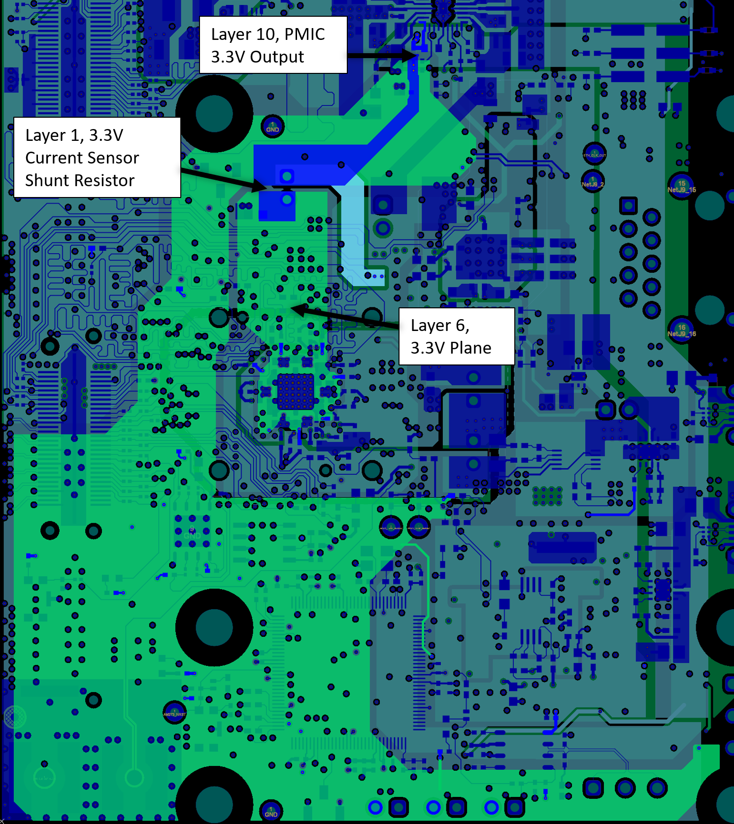
GUID-8F1314F3-D8C3-451B-B0AD-3BFF7B451986-low.png Figure 11-14 AM273 GPEVM Excerpt – 3.3 V Digital and Analog Power Planes on Layer 6
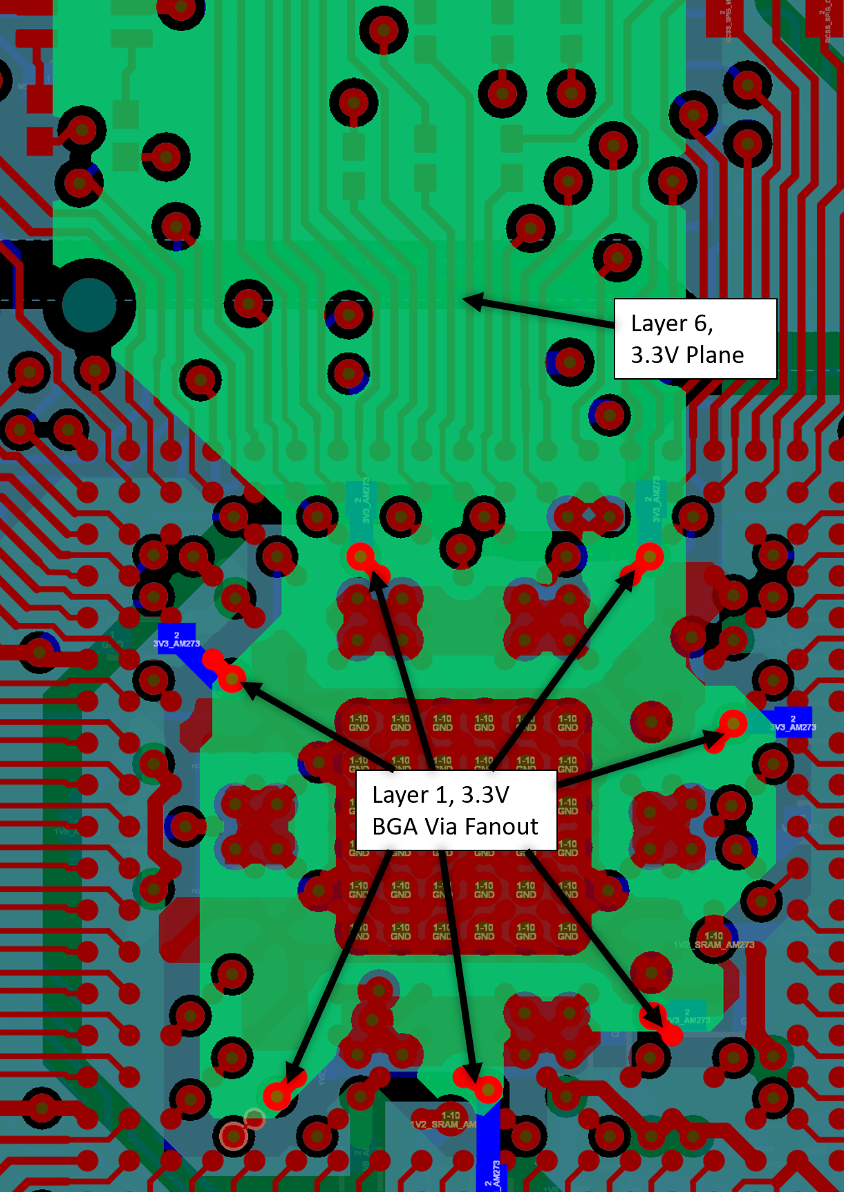
GUID-CB7128FD-1034-4D93-9F5B-F2CF4205FB89-low.png Figure 11-15 AM273 GPEVM Excerpt – 3.3 V Digital I/O and Analog I/O BGA Pinout
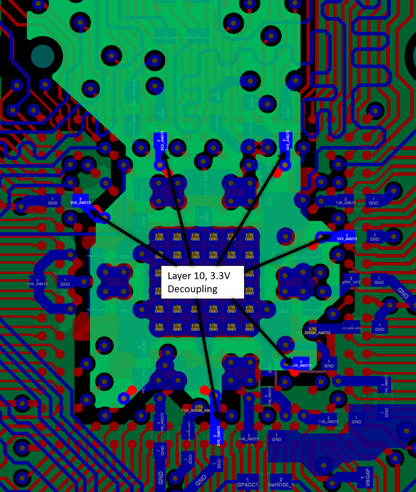
GUID-B78B31C8-4066-456E-B277-47B31CE6E1CF-low.png Figure 11-16 AM273 GPEVM Excerpt – 3.3 V Decoupling