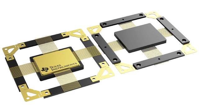
Packaging information
| Package | Pins CFP (HFG) | 76 |
| Operating temperature range (°C) -55 to 125 |
| Package qty | Carrier 1 | JEDEC TRAY (5+1) |
Features for the SMV512K32-SP
- 20-ns Read, 13.8-ns Write Through Maximum Access Time
- Functionally Compatible With Commercial
512K x 32 SRAM Devices - Built-In EDAC (Error Detection and Correction) to Mitigate Soft Errors
- Built-In Scrub Engine for Autonomous Correction
- CMOS Compatible Input and Output Level, Three State Bidirectional
Data Bus- 3.3 ±0.3-V I/O, 1.8 ±0.15-V CORE
- Radiation Performance(1)
- Uses Both Substrate Engineering and Radiation Hardened by Design (HBD)(2)
- TID Immunity > 3e5 rad (Si)
- SER < 5e-17 Upsets/Bit-Day (Core Using EDAC and Scrub)(3)
- Latch up immunity > LET = 110 MeV (T = 398K)
(1) Radiation tolerance is a typical value based upon initial device qualification. Radiation Data and Lot Acceptance Testing is available – contact factory for details.
(2) HardSIL™ technology and memory design under a license
agreement with Silicon Space Technology (SST).
(3) SER calculated using CREME96 for geosynchronous orbit,
solar minimum.
(4) These units are intended for engineering evaluation only. They are processed to a non-compliant flow (e.g. no burn-in, etc.) and are tested to temperature rating of 25°C only. These units are not suitable for qualification, production, radiation testing or flight use. Parts are not warranted for performance on full MIL specified temperature range of –55°C to 125°C or operating life.
Description for the SMV512K32-SP
The SMV512K32 is a high performance asynchronous CMOS SRAM organized as 524,288 words by 32 bits. It is pin selectable between two modes: master or slave. The master device selection provides user defined autonomous EDAC scrubbing options. The slave device selection employs a scrub on demand feature that can be initiated by a master device. Three read cycles and four write cycles (described below) are available depending on the user needs.