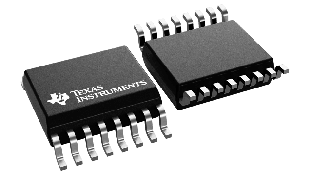
16-pin (DBQ) package image

SN74CB3Q3253DBQR ACTIVE

3.3-V, 4:1, 2-channel FET Bus Switch

ACTIVE custom-reels CUSTOM Custom reel may be available

Pricing

Qty Price
+

Quality information

Rating Catalog
RoHS Yes
REACH Yes
Lead finish / Ball material NIPDAU
MSL rating / Peak reflow Level-2-260C-1 YEAR
Quality, reliability
& packaging information

Information included:

  • RoHS
  • REACH
  • Device marking
  • Lead finish / Ball material
  • MSL rating / Peak reflow
  • MTBF/FIT estimates
  • Material content
  • Qualification summary
  • Ongoing reliability monitoring
View or download
Additional manufacturing information

Information included:

  • Fab location
  • Assembly location
View

Export classification

*For reference only

  • US ECCN: EAR99

Packaging information

Package | Pins SSOP (DBQ) | 16
Operating temperature range (°C) -40 to 85
Package qty | Carrier 2,500 | LARGE T&R

Features for the SN74CB3Q3253

  • High-Bandwidth Data Path (Up to 500 MHz) (1)
  • 5-V Tolerant I/Os With Device Powered Up or Powered Down
  • Low and Flat ON-State Resistance (ron) Characteristics Over Operating Range (ron = 4 Ω Typical)
  • Rail-to-Rail Switching on Data I/O Ports
    • 0- to 5-V Switching With 3.3-V VCC
    • 0- to 3.3-V Switching With 2.5-V VCC
  • Bidirectional Data Flow With Near-Zero Propagation Delay
  • Low Input/Output Capacitance Minimizes Loading and Signal Distortion (Cio(OFF) = 3.5 pF Typical)
  • Fast Switching Frequency (fOE = 20 MHz Max)
  • Data and Control Inputs Provide Undershoot Clamp Diodes
  • Low Power Consumption (ICC = 0.6 mA Typical)
  • VCC Operating Range From 2.3 V to 3.6 V
  • Data I/Os Support 0- to 5-V Signal Levels (0.8-V, 1.2-V, 1.5-V, 1.8-V, 2.5-V, 3.3-V, 5-V)
  • Control Inputs Can be Driven by TTL or 5-V and 3.3-V CMOS Outputs
  • Ioff Supports Partial-Power-Down Mode Operation
  • Latch-Up Performance Exceeds 100 mA Per JESD 78, Class II
  • ESD Performance Tested Per JESD 22
    • 2000-V Human-Body Model (A114-B, Class II)
    • 1000-V Charged-Device Model (C101)
  • Supports Both Digital and Analog Applications: USB Interface, Differential Signal Interface Bus Isolation, Low-Distortion Signal Gating (1)

(1) For additional information regarding the performance characteristics of the CB3Q family, refer to the TI application report CBT-C, CB3T, and CB3Q Signal-Switch Families, (SCDA008).

Description for the SN74CB3Q3253

The SN74CB3Q3253 device is a high-bandwidth FET bus switch using a charge pump to elevate the gate voltage of the pass transistor, providing a low and flat ON-state resistance (ron). The low and flat ON-state resistance allows for minimal propagation delay and supports rail-to-rail switching on the data input and output (I/O) ports.
Pricing

Qty Price
+

Carrier options

You can choose different carrier options based on the quantity of parts, including full reel, custom reel, cut tape, tube or tray.

A custom reel is a continuous length of cut tape from one reel to maintain lot- and date-code traceability, built to the exact quantity requested. Following industry standards, a brass shim connects an 18-inch leader and trailer on both sides of the cut tape for direct feeding into automated assembly machines. TI includes a reeling fee for custom reel orders.

Cut tape is a length of tape cut from a reel. TI may fulfill orders using multiple strips of cut tapes or boxes to satisfy the quantity requested.

TI often ships tube or tray devices inside a box or in the tube or tray, depending on inventory availability. We pack all tapes, tubes or sample boxes according to internal electrostatic discharge and moisture-sensitivity-level protection requirements.

Learn more

Lot and date code selection may be available

Add a quantity to your cart and begin the checkout process to view the options available to select lot or date codes from existing inventory.

Learn more