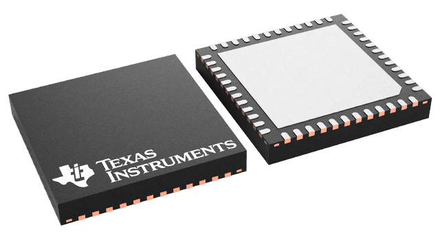
Packaging information
| Package | Pins VQFN (RGZ) | 48 |
| Operating temperature range (°C) -40 to 85 |
| Package qty | Carrier 250 | SMALL T&R |
Features for the ADC34J45
- Quad Channel
- 14-Bit Resolution
- Single 1.8-V Supply
- Flexible Input Clock Buffer with Divide-by-1, -2, -4
- SNR = 72 dBFS, SFDR = 86 dBc at
fIN = 70 MHz - Ultra-Low Power Consumption:
- 203 mW/Ch at 160 MSPS
- Channel Isolation: 105 dB
- Internal Dither
- JESD204B Serial Interface:
- Supports Subclass 0, 1, 2
- Supports One Lane per ADC up to 160 MSPS
- Support for Multi-Chip Synchronization
- Pin-to-Pin Compatible with 12-Bit Version
- Package: VQFN-48 (7 mm × 7 mm)
Description for the ADC34J45
The ADC34J4x is a high-linearity, ultra-low power, quad-channel, 14-bit, 50-MSPS to 160-MSPS, analog-to-digital converter (ADC). The devices are designed specifically to support demanding, high input frequency signals with large dynamic range requirements. A clock input divider allows more flexibility for system clock architecture design while the SYSREF input enables complete system synchronization. The ADC34J4x family supports serial current-mode logic (CML) and JESD204B interfaces in order to reduce the number of interface lines, thus allowing high system integration density. The JESD204B interface is a serial interface, where the data of each ADC are serialized and output over only one differential pair. An internal phase-locked loop (PLL) multiplies the incoming ADC sampling clock by 20 to derive the bit clock that is used to serialize the 14-bit data from each channel. The ADC34J4x devices support subclass 1 with interface speeds up to 3.2 Gbps.