Packaging information
| Package | Pins VQFN (RGT) | 16 |
| Operating temperature range (°C) -40 to 85 |
| Package qty | Carrier 250 | SMALL T&R |
Features for the THS4520
- Fully Differential Architecture With Rail-to-Rail Outputs
- Centered Input Common-mode Range
- Minimum Gain of 1 V/V (0 dB)
- Bandwidth: 620 MHz
- Slew Rate: 570 V/µs
- 0.1% Settling Time: 7 ns
- HD2: –115 dBc at 100 kHz, VOD = 8 VPP
- HD3: –123 dBc at 100 kHz, VOD = 8 VPP
- Input Voltage Noise: 2 nV/
 Hz (f >10 kHz)
 - Output Common-Mode Control
- Power Supply:
- Voltage: 3.3 V (±1.65 V) to 5 V (±2.5 V)
- Current: 14.2 mA
- Power-Down Capability: 15 µA
- APPLICATIONS
- 5-V and 3.3-V Data Acquisition Systems
- High Linearity ADC Amplifier
- Wireless Communication
- Test and Measurement
- Voice Processing Systems
Description for the THS4520
The THS4520 is a wideband, fully differential operational amplifier designed for 5-V data acquisition systems. It has very low noise at 2 nV/ load. The slew rate is 570 V/µs, and with a settling time of 7 ns to 0.1% (2-V step), it is ideal for data acquisition applications. It is designed for unity gain stability.
To allow for dc coupling to ADCs, its unique output common-mode control circuit maintains the output common-mode voltage within 0.25 mV offset (typical) from the set voltage. The common-mode set point defaults to mid-supply by internal circuitry, which may be over-driven from an external source.
The input and output are optimized for best performance with their common-mode voltages set to mid-supply. Along with high performance at low power supply voltage, this makes for extremely high performance single supply 5-V and 3.3-V data acquisition systems.
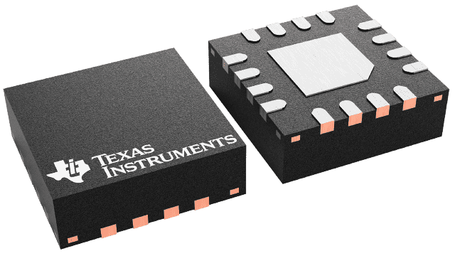
The THS4520 is offered in a Quad 16-pin leadless QFN package (RGT), and is characterized for operation over the full industrial temperature range from –40°C to 85°C.