JAJSP34G October 2011 – September 2022 TPS40422
PRODUCTION DATA
- 1 特長
- 2 アプリケーション
- 3 概要
- 4 Revision History
- 5 概要 (続き)
- 6 Pin Configuration and Functions
- 7 Specifications
-
8 Detailed Description
- 8.1 Overview
- 8.2 Functional Block Diagram
- 8.3
Feature Description
- 8.3.1 PMBus Interface Protocol General Description
- 8.3.2 Voltage Reference
- 8.3.3 Output Voltage
- 8.3.4 Voltage Feed Forward
- 8.3.5 Current Sensing
- 8.3.6 Overcurrent Protection
- 8.3.7 Current Sharing
- 8.3.8 Linear Regulators
- 8.3.9 BP Switch-over
- 8.3.10 Switching Frequency Setting
- 8.3.11 Switching Node and BOOT Voltage
- 8.3.12 Reading the Output Current
- 8.3.13 Soft-Start Time
- 8.3.14 Turn-On/Turn-Off Delay and Sequencing
- 8.3.15 Pre-Biased Output Start-Up
- 8.3.16 Undervoltage Lockout
- 8.3.17 Overvoltage and Undervoltage Fault Protection
- 8.3.18 Power Good
- 8.3.19 Overtemperature Fault Protection
- 8.3.20 Thermal Shutdown
- 8.3.21 Programmable Fault Responses
- 8.3.22 User Data
- 8.3.23 Adjustable Anti-Cross Conduction Delay
- 8.3.24 Connection of Unused Pins
- 8.4 Device Functional Modes
- 8.5 Programming
- 8.6
Register Maps
- 8.6.1
Supported Commands
- 8.6.1.1 PAGE (00h)
- 8.6.1.2 OPERATION (01h)
- 8.6.1.3 ON_OFF_CONFIG (02h)
- 8.6.1.4 CLEAR_FAULTS (03h)
- 8.6.1.5 WRITE_PROTECT (10h)
- 8.6.1.6 STORE_USER_ALL (15h)
- 8.6.1.7 RESTORE_USER_ALL (16h)
- 8.6.1.8 CAPABILITY (19h)
- 8.6.1.9 VOUT_MODE (20h)
- 8.6.1.10 VIN_ON (35h)
- 8.6.1.11 VIN_OFF (36h)
- 8.6.1.12 IOUT_CAL_GAIN (38h)
- 8.6.1.13 IOUT_CAL_OFFSET (39h)
- 8.6.1.14 IOUT_OC_FAULT_LIMIT (46h)
- 8.6.1.15 IOUT_OC_FAULT_RESPONSE (47h)
- 8.6.1.16 IOUT_OC_WARN_LIMIT (4Ah)
- 8.6.1.17 OT_FAULT_LIMIT (4Fh)
- 8.6.1.18 OT_WARN_LIMIT (51h)
- 8.6.1.19 TON_RISE (61h)
- 8.6.1.20 STATUS_BYTE (78h)
- 8.6.1.21 STATUS_WORD (79h)
- 8.6.1.22 STATUS_VOUT (7Ah)
- 8.6.1.23 STATUS_IOUT (7Bh)
- 8.6.1.24 STATUS_TEMPERATURE (7Dh)
- 8.6.1.25 STATUS_CML (7Eh)
- 8.6.1.26 STATUS_MFR_SPECIFIC (80h)
- 8.6.1.27 READ_VOUT (8Bh)
- 8.6.1.28 READ_IOUT (8Ch)
- 8.6.1.29 READ_TEMPERATURE_2 (8Eh)
- 8.6.1.30 PMBUS_REVISION (98h)
- 8.6.1.31 MFR_SPECIFIC_00 (D0h)
- 8.6.1.32 VREF_TRIM (MFR_SPECIFIC_04) (D4h)
- 8.6.1.33 STEP_VREF_MARGIN_HIGH (MFR_SPECIFIC_05) (D5h)
- 8.6.1.34 STEP_VREF_MARGIN_LOW (MFR_SPECIFIC_06) (D6h)
- 8.6.1.35 PCT_VOUT_FAULT_PG_LIMIT (MFR_SPECIFIC_07) (D7h)
- 8.6.1.36 126
- 8.6.1.37 SEQUENCE_TON_TOFF_DELAY (MFR_SPECIFIC_08) (D8h)
- 8.6.1.38 128
- 8.6.1.39 OPTIONS (MFR_SPECIFIC_21) (E5h)
- 8.6.1.40 DEVICE_CODE (MFR_SPECIFIC_44) (FCh)
- 8.6.1
Supported Commands
-
9 Application and Implementation
- 9.1 Application Information
- 9.2
Typical Application
- 9.2.1
Dual-Output Converter
- 9.2.1.1 Design Requirements
- 9.2.1.2
Detailed Design Procedure
- 9.2.1.2.1 Custom Design with WEBENCH® Tools
- 9.2.1.2.2 Step 1: Inductor Selection
- 9.2.1.2.3 Step 2: Output Capacitor Selection
- 9.2.1.2.4 Step 3: Input Capacitance Selection
- 9.2.1.2.5 Step 4: MOSFET Selection
- 9.2.1.2.6 Step 5: Snubber Circuit Design
- 9.2.1.2.7 Step 6: Soft-Start Time
- 9.2.1.2.8
Step 7: Peripheral Component Design
- 9.2.1.2.8.1 RT (Pin 1) Switching Frequency Setting
- 9.2.1.2.8.2 FB1 (Pin 2) and FB2 (Pin 8) Output Voltage Setting
- 9.2.1.2.8.3 Compensation Network Using COMP1 (Pin 3) , COMP2 (Pin 7), FB1 (Pin 2) FB2 DIFFO1 (Pin 8) (Pin 39)
- 9.2.1.2.8.4 Remote Sensing Using VSNS1 (Pin 37), GSNS1 (Pin 38) , VSNS2 (Pin 15), and GSNS2 (Pin 14)
- 9.2.1.2.8.5 Temperate Sensing Using TSNS1 (Pin36) and TSNS2 (Pin 16)
- 9.2.1.2.8.6 Current Sensing Network Design Using CS1P (Pin 34), CS1N (Pin 35) , CS2P (Pin 18), and CS2N (Pin 17)
- 9.2.1.2.8.7 PMBus Address ADDR1 (Pin 9) , and ADDR0 (Pin 10)
- 9.2.1.2.8.8
Voltage Decoupling Capacitors
- 9.2.1.2.8.8.1 VDD (Pin 31)
- 9.2.1.2.8.8.2 BP3 (Pin 32)
- 9.2.1.2.8.8.3 BNEXT (Pin 24)
- 9.2.1.2.8.8.4 BP6 (Pin 25)
- 9.2.1.2.8.8.5 Power Good PGOOD1 (Pin 33), PGOOD2 (Pin 19)
- 9.2.1.2.8.8.6 Bootstrap Capacitors BOOT1 (Pin 30), and BOOT2 (Pin 20)
- 9.2.1.2.8.8.7 High-Side MOSFET (Gate) Resistor
- 9.2.1.2.8.8.8 Synchronization Setting SYNC (Pin 40)
- 9.2.1.2.8.8.9 BP6 (Pin 25)
- 9.2.1.2.8.8.10 DIFFO (Pin 39)
- 9.2.1.3 Application Curves
- 9.2.1
Dual-Output Converter
- 10Power Supply Recommendations
- 11Layout
- 12Device and Documentation Support
- 13Mechanical, Packaging, and Orderable Information
パッケージ・オプション
メカニカル・データ(パッケージ|ピン)
サーマルパッド・メカニカル・データ
発注情報
8.3.13 Soft-Start Time
The TPS4022 device supports several soft-start times between 600 μs and 9 ms. Use the TON_RISE PMBus command to select the soft-start time. See the Section 8.6.1.19 command description for full details on the levels and implementation. When selecting the soft-start time, carefully consider the charging current for the output capacitors. In some applications (for example, those with large amounts of output capacitance) this current level can lead to problems with nuisance tripping of the overcurrent protection circuitry. To ensure that this does not happen, include a consideration of the output capacitor charging current when choosing the overcurrent threshold setting. Use Equation 6 to calculate the output capacitor charging current.
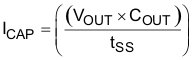
where
- ICAP is the startup charging current of the output capacitance in A
- VOUT is the output voltage of the converter in V
- COUT is the total output capacitance in F
- tSS is the selected soft-start time in seconds
After calculating the charging current, the overcurrent threshold can then be calibrated to the sum of the maximum load current and the output capacitor charging current plus some margin. The amount of margin required depends on the individual application, but 25% is a suggested starting point. Individual applications may require more or less than 25%.