SLOA011B January 2018 – July 2021 LF347 , LF353 , LM348 , MC1458 , TL022 , TL061 , TL062 , TL071 , TL072 , UA741
- 1Introduction
- 2Non-Inverting Amplifier
- 3Inverting Amplifier
- 4Simplified Op Amp Circuit Diagram
-
5Op Amp Specifications
- 5.1 Absolute Maximum Ratings and Recommended Operating Condition
- 5.2 Input Offset Voltage
- 5.3 Input Current
- 5.4 Input Common Mode Voltage Range
- 5.5 Differential Input Voltage Range
- 5.6 Maximum Output Voltage Swing
- 5.7 Large Signal Differential Voltage Amplification
- 5.8 Input Parasitic Elements
- 5.9 Output Impedance
- 5.10 Common-Mode Rejection Ratio
- 5.11 Supply Voltage Rejection Ratio
- 5.12 Supply Current
- 5.13 Slew Rate at Unity Gain
- 5.14 Equivalent Input Noise
- 5.15 Total Harmonic Distortion Plus Noise
- 5.16 Unity-Gain Bandwidth and Phase Margin
- 5.17 Settling Time
- 6References
- 7Glossary
- 8Revision History
1.2 Ideal Op Amp Model
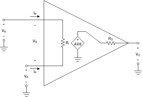
The Thevenin amplifier model shown in Figure 1-1 is redrawn in Figure 1-2 showing standard op amp notation. An op amp is a differential to single-ended amplifier. It amplifies the voltage difference, Vd = Vp - Vn, on the input port and produces a voltage, Vo, on the output port that is referenced to ground.
 Figure 1-2 Standard Op Amp Notation
We still have the loading effects at the input and output ports as noted above. The ideal op amp model was derived to simplify circuit calculations and is commonly used by engineers in first-order approximation calculations. The ideal model makes three simplifying assumptions:
- Gain is infinite
Equation 1. a = ∞
- Input resistance is infinite
Equation 2. Ri = ∞
- Output resistance is zero
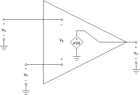
Equation 3. Ro = 0
Applying these assumptions to Figure 1-2 results in the ideal op amp model shown in Figure 1-3.
 Figure 1-3 Ideal Op Amp Model
Other simplifications can be derived using the ideal op amp model:
Because Ri = ∞, we assume In = Ip = 0. There is no loading effect at the input.
Because Ro = 0 there is no loading effect at the output.
If the op amp is in linear operation, V0 must be a finite voltage. By definition Vo = Vd × a. Rearranging, Vd = Vo / a . Since a = ∞, Vd = Vo / ∞ = 0. This is the basis of the virtual short concept.
The ideal voltage source driving the output port depends only on the voltage difference across its input port. It rejects any voltage common to Vn and Vp.
No frequency dependencies are assumed.
There are no changes in performance over time, temperature, humidity, power supply variations, etc.