SLOA011B January 2018 – July 2021 LF347 , LF353 , LM348 , MC1458 , TL022 , TL061 , TL062 , TL071 , TL072 , UA741
- 1Introduction
- 2Non-Inverting Amplifier
- 3Inverting Amplifier
- 4Simplified Op Amp Circuit Diagram
-
5Op Amp Specifications
- 5.1 Absolute Maximum Ratings and Recommended Operating Condition
- 5.2 Input Offset Voltage
- 5.3 Input Current
- 5.4 Input Common Mode Voltage Range
- 5.5 Differential Input Voltage Range
- 5.6 Maximum Output Voltage Swing
- 5.7 Large Signal Differential Voltage Amplification
- 5.8 Input Parasitic Elements
- 5.9 Output Impedance
- 5.10 Common-Mode Rejection Ratio
- 5.11 Supply Voltage Rejection Ratio
- 5.12 Supply Current
- 5.13 Slew Rate at Unity Gain
- 5.14 Equivalent Input Noise
- 5.15 Total Harmonic Distortion Plus Noise
- 5.16 Unity-Gain Bandwidth and Phase Margin
- 5.17 Settling Time
- 6References
- 7Glossary
- 8Revision History
5.13 Slew Rate at Unity Gain
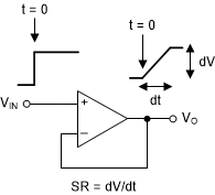
Slew rate, SR, is the rate of change in the output voltage caused by a step input. Its units are V/us or V/ms. Figure 5-8 shows slew rate graphically.
Referring back to Figure 4-1, voltage change in the second stage is limited by the charging and discharging of capacitor Cc. The maximum rate of change occurs when either side of the differential pair is conducting 2IE. This is the major limit to slew rate. Essentially, SR = 2IE/Cc. However, there are op amps that work on different principles where this is not true.
The requirement to have current flowing in or out of the input stage to change the voltage out of the second stage requires an error voltage at the input anytime the output voltage of an op amp is changing. An error voltage on the order of 120 mV is required for an op amp with a bipolar input to realize full slew rate. This can be as high as 1 V to 3 V for a JFET or MOSFET input.
Capacitor, Cc, is added to make the op amp unity gain stable. Some op amps come in de-compensated versions where the value of Cc is reduced . This increases realizable bandwidth and slew rate, but the engineer must ensure the stability of the circuit by other means.
In op amps you trade power consumption for noise and speed. To increase slew rate, the bias currents within the op amp are increased.
 Figure 5-8 Slew Rate