SLOA011B January 2018 – July 2021 LF347 , LF353 , LM348 , MC1458 , TL022 , TL061 , TL062 , TL071 , TL072 , UA741
- 1Introduction
- 2Non-Inverting Amplifier
- 3Inverting Amplifier
- 4Simplified Op Amp Circuit Diagram
-
5Op Amp Specifications
- 5.1 Absolute Maximum Ratings and Recommended Operating Condition
- 5.2 Input Offset Voltage
- 5.3 Input Current
- 5.4 Input Common Mode Voltage Range
- 5.5 Differential Input Voltage Range
- 5.6 Maximum Output Voltage Swing
- 5.7 Large Signal Differential Voltage Amplification
- 5.8 Input Parasitic Elements
- 5.9 Output Impedance
- 5.10 Common-Mode Rejection Ratio
- 5.11 Supply Voltage Rejection Ratio
- 5.12 Supply Current
- 5.13 Slew Rate at Unity Gain
- 5.14 Equivalent Input Noise
- 5.15 Total Harmonic Distortion Plus Noise
- 5.16 Unity-Gain Bandwidth and Phase Margin
- 5.17 Settling Time
- 6References
- 7Glossary
- 8Revision History
5.6 Maximum Output Voltage Swing
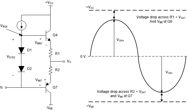
The maximum output voltage, VOM±, is defined as “the maximum positive or negative peak output voltage that can be obtained without wave form clipping when quiescent DC output voltage is zero”. VOM± is limited by the output impedance of the amplifier, the saturation voltage of the output transistors, and the power supply voltages. This is shown in Figure 5-5. Note that VOM± depends on the output load.
 Figure 5-5 VOM±
The maximum value that VBQ6 can be is +VCC, therefore VO ≤ +VCC – VR1 – VBEQ6 – VSATQ6. The minimum value that Vi can be is –VEE, therefore VO ≥ –VEE + VR2 + VBEQ7 + VSATQ7.
This emitter follower structure cannot drive the output voltage to either rail. Rail to rail output op amps use a common emitter (bipolar) or common source (CMOS) output stage. With these structures, the output voltage swing is only limited by the saturation voltage (bipolar) or the on resistance (CMOS) of the output transistors, and the load being driven.
Because newer products are focused on single supply operation, more recent data sheets from Texas Instruments use the terminology VOH and VOL to specify the maximum and minimum output voltage.
Maximum and minimum output voltage is usually a design issue when dynamic range is lost if the op amp cannot drive to the rails. This is the case in single supply systems where the op amp is used to drive the input of an analog-to-digital converter, which is configured for full scale input voltage between ground and the positive rail.