SLOA011B January 2018 – July 2021 LF347 , LF353 , LM348 , MC1458 , TL022 , TL061 , TL062 , TL071 , TL072 , UA741
- 1Introduction
- 2Non-Inverting Amplifier
- 3Inverting Amplifier
- 4Simplified Op Amp Circuit Diagram
-
5Op Amp Specifications
- 5.1 Absolute Maximum Ratings and Recommended Operating Condition
- 5.2 Input Offset Voltage
- 5.3 Input Current
- 5.4 Input Common Mode Voltage Range
- 5.5 Differential Input Voltage Range
- 5.6 Maximum Output Voltage Swing
- 5.7 Large Signal Differential Voltage Amplification
- 5.8 Input Parasitic Elements
- 5.9 Output Impedance
- 5.10 Common-Mode Rejection Ratio
- 5.11 Supply Voltage Rejection Ratio
- 5.12 Supply Current
- 5.13 Slew Rate at Unity Gain
- 5.14 Equivalent Input Noise
- 5.15 Total Harmonic Distortion Plus Noise
- 5.16 Unity-Gain Bandwidth and Phase Margin
- 5.17 Settling Time
- 6References
- 7Glossary
- 8Revision History
5.2 Input Offset Voltage
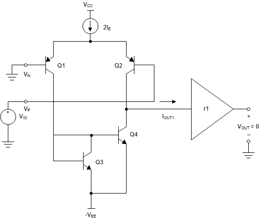
Input offset voltage, VIO, is defined as "the DC voltage that must be applied between the input terminals to force the quiescent DC output voltage to zero or some other level, if specified". If the input stage was perfectly symmetrical and the transistors were perfectly matched, VIO = 0. Because of process variations, geometry and doping are never exact to the last detail. All op amps require a small voltage between their inverting and non-inverting inputs to balance the mismatches. VIO is normally depicted as a voltage source driving the non-inverting input, as shown in Figure 5-1.
TI data sheets show two other parameters related to VIO; the average temperature coefficient of the input offset voltage and the input offset voltage long-term drift.
The average temperature coefficient of input offset voltage, αVIO, specifies the expected input offset drift over temperature. Its units are uV/°C. VIO is measured at the temperature extremes of the part, and αVIO is computed as ΔVIO/Δ°C.
Normal aging in semiconductors causes changes in the characteristics of devices. The input offset voltage long-term drift specifies how VIO is expected to change with time. Its units are mV/month.
 Figure 5-1 VIO
Input offset voltage is of concern anytime DC precision is required. Several methods are used to null its effects.