SBOS671D September 2018 – December 2022 OPA2828 , OPA828
PRODUCTION DATA
- 1 Features
- 2 Applications
- 3 Description
- 4 Revision History
- 5 Pin Configuration and Functions
- 6 Specifications
-
7 Detailed Description
- 7.1 Overview
- 7.2 Functional Block Diagram
- 7.3
Feature Description
- 7.3.1 Phase-Reversal Protection
- 7.3.2 Electrical Overstress
- 7.3.3 MUX Friendly Inputs
- 7.3.4 Overload Power Limiter
- 7.3.5 Noise Performance
- 7.3.6 Capacitive Load and Stability
- 7.3.7 Settling Time
- 7.3.8 Slew Rate
- 7.3.9 Full-Power Bandwidth
- 7.3.10 Small-Signal Response
- 7.3.11 Thermal Shutdown
- 7.3.12 Low Offset Voltage Drift
- 7.3.13 Overload Recovery
- 7.4 Device Functional Modes
- 8 Application and Implementation
- 9 Device and Documentation Support
- 10Mechanical, Packaging, and Orderable Information
Package Options
Mechanical Data (Package|Pins)
Thermal pad, mechanical data (Package|Pins)
- DGN|8
Orderable Information
6.6 Typical Characteristics
At TA = 25°C, RL = 2 kΩ connected to midsupply, and VCM = VOUT = midsupply, and VS = ±18 V (unless otherwise noted)
Table 6-1 Table of Graphs
| DESCRIPTION | FIGURE |
|---|---|
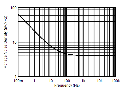
| Input Voltage Noise Density vs Frequency | Figure 6-1 |
| . Integrated Input Voltage Noise vs Bandwidth | Figure 6-2 |
| Total Harmonic Distortion + Noise Ratio vs Frequency | Figure 6-3 |
| Total Harmonic Distortion + Noise Ratio vs Output Amplitude | Figure 6-4 |
| . 0.1-Hz To 10-Hz Noise | Figure 6-5 |
| Offset Voltage Production Distribution | Figure 6-6, Figure 6-7 |
| Offset Voltage Drift Production Distribution | Figure 6-8, Figure 6-9 |
| Offset Voltage vs Common-Mode Voltage | Figure 6-10 |
| Offset Voltage vs Power Supply Voltage | Figure 6-11 |
| Offset Voltage vs Output Voltage | Figure 6-12 |
| . Offset Voltage vs Temperature | Figure 6-13 |
| Input Bias and Input Offset Current vs Common-Mode Voltage | Figure 6-14 |
| Input Bias and Input Offset Current vs Temperature | Figure 6-15 |
| Quiescent Current vs Output Voltage | Figure 6-16 |
| Quiescent Current vs Temperature | Figure 6-17 |
| Output Voltage Swing vs Output Sourcing Current | Figure 6-18 |
| Output Voltage Swing vs Output Sinking Current | Figure 6-19 |
| Power-Supply Rejection Ratio vs Frequency | Figure 6-20 |
| Common-Mode Rejection Ratio vs Frequency | Figure 6-21 |
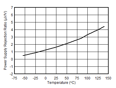
| Power-Supply Rejection Ratio vs Temperature | Figure 6-22 |
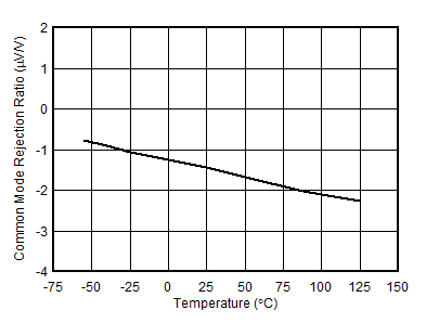
| Common-Mode Rejection Ratio vs Temperature | Figure 6-23 |
| Open-Loop Gain and Phase vs Frequency | Figure 6-24 |
| Closed-Loop Gain vs Frequency | Figure 6-25 |
| Open-Loop Gain vs Temperature | Figure 6-26 |
| Open-Loop Output Impedance vs Frequency | Figure 6-27 |
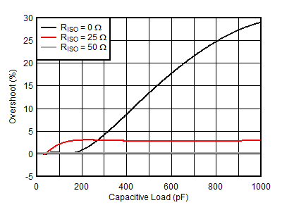
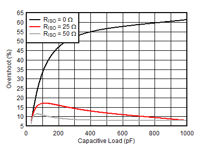
| Small-Signal Overshoot vs Capacitive Load, Gain = +1 | Figure 6-28 |
| Small-Signal Overshoot vs Capacitive Load, Gain = –1 | Figure 6-29 |
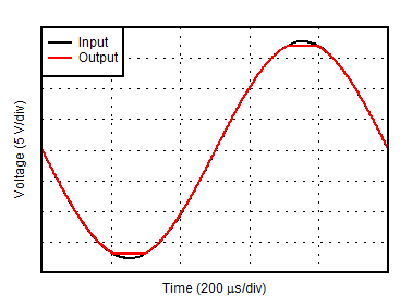
| No Phase Reversal | Figure 6-30 |
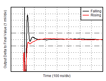
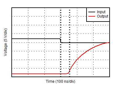
| Positive Overload Recovery | Figure 6-31 |
| Negative Overload Recovery | Figure 6-32 |
| . Small-Signal Step Response | Figure 6-33 |
| Large-Signal Step Response | Figure 6-34 |
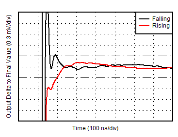
| 12-bit, 14-bit Settling Time | Figure 6-35, Figure 6-36 |
| Short-Circuit Current vs Temperature | Figure 6-37 |
| Slew Rate vs Temperature | Figure 6-38 |
| Slew Rate vs Output Step Size | Figure 6-39 |
| Maximum Output Voltage vs Frequency | Figure 6-40 |
| Intermodulation Distortion | Figure 6-41 |
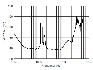
| Electromagnetic Interference Rejection | Figure 6-42 |
| Harmonic Distortion vs Frequency | Figure 6-43 |
| Channel Separation | Figure 6-44 |
| DGN package, VS = ±15 V |
| DGN package, TA = –40°C to +125°C |
| 5 typical units |
| VS = ±15 V |
| Differential amp configuration, 10-kΩ resistors |
| Gain = –1 |
| Buffer configuration |
| Noise bandwidth = 0.1 Hz to indicated frequency |
| VS = ±15 V |
| TA = –40°C to +125°C |
| VS = ±15 V, 5 typical units |
| VS = ±15 V, 5 typical units |
| VS = ±15 V |
| Gain = +1 |
| Gain = +1 |
| OPA2828, DGN package |