SBOS671D September 2018 – December 2022 OPA2828 , OPA828
PRODUCTION DATA
- 1 Features
- 2 Applications
- 3 Description
- 4 Revision History
- 5 Pin Configuration and Functions
- 6 Specifications
-
7 Detailed Description
- 7.1 Overview
- 7.2 Functional Block Diagram
- 7.3
Feature Description
- 7.3.1 Phase-Reversal Protection
- 7.3.2 Electrical Overstress
- 7.3.3 MUX Friendly Inputs
- 7.3.4 Overload Power Limiter
- 7.3.5 Noise Performance
- 7.3.6 Capacitive Load and Stability
- 7.3.7 Settling Time
- 7.3.8 Slew Rate
- 7.3.9 Full-Power Bandwidth
- 7.3.10 Small-Signal Response
- 7.3.11 Thermal Shutdown
- 7.3.12 Low Offset Voltage Drift
- 7.3.13 Overload Recovery
- 7.4 Device Functional Modes
- 8 Application and Implementation
- 9 Device and Documentation Support
- 10Mechanical, Packaging, and Orderable Information
Package Options
Mechanical Data (Package|Pins)
Thermal pad, mechanical data (Package|Pins)
- DGN|8
Orderable Information
7.3.10 Small-Signal Response
The parameters of an amplifier that best describe the small signal dynamic behavior are the gain-bandwidth product (GBP), unity gain frequency (UGF), and phase margin (PM). The GBP is a useful parameter to determine the bandwidth of an application in closed-loop configurations. Equation 4 can be used to approximate the closed loop bandwidth for the OPAx828. Typically, the GBP is a specified parameter with the amplifier configured in a noninverting gain of 100 (40 dB). The GBP of an amplifier is generally assumed to be constant over frequency but in some higher speed amplifiers, constant over frequency is not the case. The OPAx828 have a constant GBP all the way to the UGF; thus, the OPAx828 open-loop gain has a constant –20 dB/decade slope (–6 dB/octave). The UGF is defined as the frequency at which the gain of the amplifier crosses 1 V/V (0 dB). Figure 7-13 illustrates the concept of GBP and UGF. The OPAx828 have both a GBP and UGF of 45 MHz.
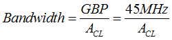
 Figure 7-13 Gain-Bandwidth Product and Unity Gain
Frequency
Figure 7-13 Gain-Bandwidth Product and Unity Gain
Frequency