SBOS671D September 2018 – December 2022 OPA2828 , OPA828
PRODUCTION DATA
- 1 Features
- 2 Applications
- 3 Description
- 4 Revision History
- 5 Pin Configuration and Functions
- 6 Specifications
-
7 Detailed Description
- 7.1 Overview
- 7.2 Functional Block Diagram
- 7.3
Feature Description
- 7.3.1 Phase-Reversal Protection
- 7.3.2 Electrical Overstress
- 7.3.3 MUX Friendly Inputs
- 7.3.4 Overload Power Limiter
- 7.3.5 Noise Performance
- 7.3.6 Capacitive Load and Stability
- 7.3.7 Settling Time
- 7.3.8 Slew Rate
- 7.3.9 Full-Power Bandwidth
- 7.3.10 Small-Signal Response
- 7.3.11 Thermal Shutdown
- 7.3.12 Low Offset Voltage Drift
- 7.3.13 Overload Recovery
- 7.4 Device Functional Modes
- 8 Application and Implementation
- 9 Device and Documentation Support
- 10Mechanical, Packaging, and Orderable Information
Package Options
Mechanical Data (Package|Pins)
Thermal pad, mechanical data (Package|Pins)
- DGN|8
Orderable Information
8.4.1.2 PowerPAD™ Design Considerations (DGN package only)
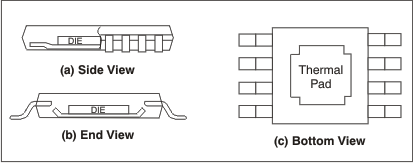
The OPAx828 are available in a thermally-enhanced, PowerPAD integrated circuit package. Figure 8-9(a) and (b) illustrate how the PowerPAD packages are constructed using a downset leadframe upon which the die is mounted. Figure 8-9(c) shows how this arrangement results in the leadframe being exposed as a thermal pad on the underside of the package. This thermal pad has direct thermal contact with the die. Therefore, excellent thermal performance is achieved by providing a good thermal path away from the thermal pad.
 Figure 8-9 Views of the
Thermally-Enhanced Package
Figure 8-9 Views of the
Thermally-Enhanced PackageThe PowerPAD integrated circuit package allows for both assembly and thermal management in one manufacturing operation. During the surface-mount solder operation (when the leads are being soldered), the thermal pad must be soldered to a copper area underneath the package. Through the use of thermal paths within this copper area, heat is conducted away from the package into either a ground plane or other heat-dissipating device. Soldering the thermal pad to the printed circuit board (PCB) is always required, even with applications that have low power dissipation. This soldering provides the necessary thermal and mechanical connection between the leadframe die pad and the PCB. Although the die is electrically isolated (>10 MΩ) from the exposed thermal pad, tie the pad to V– or a system ground plane to minimize potential leakage to the input pins. See Figure 8-11 for additional details.