SBOS671D September 2018 – December 2022 OPA2828 , OPA828
PRODUCTION DATA
- 1 Features
- 2 Applications
- 3 Description
- 4 Revision History
- 5 Pin Configuration and Functions
- 6 Specifications
-
7 Detailed Description
- 7.1 Overview
- 7.2 Functional Block Diagram
- 7.3
Feature Description
- 7.3.1 Phase-Reversal Protection
- 7.3.2 Electrical Overstress
- 7.3.3 MUX Friendly Inputs
- 7.3.4 Overload Power Limiter
- 7.3.5 Noise Performance
- 7.3.6 Capacitive Load and Stability
- 7.3.7 Settling Time
- 7.3.8 Slew Rate
- 7.3.9 Full-Power Bandwidth
- 7.3.10 Small-Signal Response
- 7.3.11 Thermal Shutdown
- 7.3.12 Low Offset Voltage Drift
- 7.3.13 Overload Recovery
- 7.4 Device Functional Modes
- 8 Application and Implementation
- 9 Device and Documentation Support
- 10Mechanical, Packaging, and Orderable Information
Package Options
Mechanical Data (Package|Pins)
Thermal pad, mechanical data (Package|Pins)
- DGN|8
Orderable Information
7.3.4 Overload Power Limiter
Many applications have tight limits on op-amp power consumption; therefore, amplifier power consumption must remain constant, even during fault conditions such as a large voltage across the inputs or the output hitting the rail. In particular, high slew-rate amplifiers such as the OPAx828 temporarily increase the supply current when the amplifier is slewing. In slew-boosted amplifiers, the presence of a large input signal can present a specific problem because the large input signal applies a large voltage across the amplifier inputs. This large voltage across the inputs activates the slew-boost and can lead to a significant increase in current consumption. At high supply voltages, the large current consumption can lead to significant amplifier self-heating.
The OPAx828 offer a high slew rate of 150 V/us in combination with a low supply current of 5.5 mA. Like many other amplifiers, these characteristics are achieved by a slew-boosting method, which temporarily increases the amplifier current consumption when the amplifier is slewing. Such a slewing condition is detected by measuring the voltage across the input pins. In a quiescent condition, this voltage is very small (equal to the amplifier offset). Alternatively, if an input voltage is changed rapidly, a large voltage is applied across the inputs and the amplifier output must slew. On the OPAx828, the supply current increase is gradual and proportional to the applied input voltage, providing a well-behaved large step response and excellent THD. The high slew rate makes sure the output resettles in less than about 300 ns; therefore, the increased power consumption is absorbed by the decoupling capacitors, and does not additionally load the power supplies.
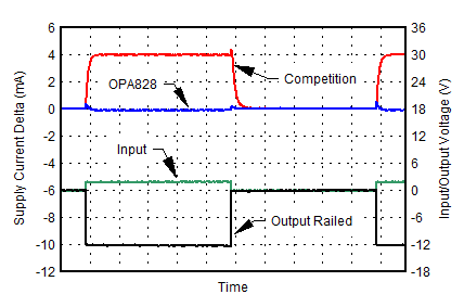
In the OPAx828, such an increase in current consumption is avoided by an additional protection circuit that continuously monitors both the amplifier inputs and output. If a large input voltage is detected, the protection circuit checks for the presence of a rapid change in voltage at the output. If the output voltage is not changing (for example, because the output is at supply rails), the protection circuit disables the slew-boost circuit after a delay of approximately 300 ns. After the overload condition is removed, the amplifier rapidly recovers to a normal operating condition. This operation is shown in Figure 7-6, where the amplifiers supply current is measured with decoupling capacitors removed. After 300 ns, the power consumption of the amplifier returns to quiescent levels. At the same time, the amplifier still has an excellent overload recovery time of < 55 ns.
