SBOS671D September 2018 – December 2022 OPA2828 , OPA828
PRODUCTION DATA
- 1 Features
- 2 Applications
- 3 Description
- 4 Revision History
- 5 Pin Configuration and Functions
- 6 Specifications
-
7 Detailed Description
- 7.1 Overview
- 7.2 Functional Block Diagram
- 7.3
Feature Description
- 7.3.1 Phase-Reversal Protection
- 7.3.2 Electrical Overstress
- 7.3.3 MUX Friendly Inputs
- 7.3.4 Overload Power Limiter
- 7.3.5 Noise Performance
- 7.3.6 Capacitive Load and Stability
- 7.3.7 Settling Time
- 7.3.8 Slew Rate
- 7.3.9 Full-Power Bandwidth
- 7.3.10 Small-Signal Response
- 7.3.11 Thermal Shutdown
- 7.3.12 Low Offset Voltage Drift
- 7.3.13 Overload Recovery
- 7.4 Device Functional Modes
- 8 Application and Implementation
- 9 Device and Documentation Support
- 10Mechanical, Packaging, and Orderable Information
Package Options
Mechanical Data (Package|Pins)
Thermal pad, mechanical data (Package|Pins)
- DGN|8
Orderable Information
8.4.1.1 Thermal Considerations
Through normal operation, the OPAx828 self-heat. Self-heating is a natural increase in the die junction temperature that occurs in every amplifier. This self-heating is a result of several factors, including quiescent power consumption, package thermal resistance, PCB layout, and device operating conditions.
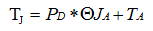
To make sure that the amplifier operates without entering thermal shutdown, use Equation 7 to calculate the approximate junction (die) temperature:
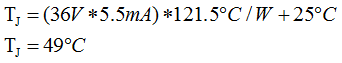
As an example, Equation 8 calculates the approximate junction temperature for the OPA828 (D package) while unloaded with an ambient temperature of 25°C.
For high-voltage, high-precision amplifiers, such as the OPAx828, the junction temperature can easily be tens of degrees higher than the ambient temperature in a quiescent (unloaded) condition. As shown by Equation 7 and Equation 8, the junction temperature depends on the thermal properties of the package, as expressed by the junction-to-ambient thermal resistance (RϴJA). If the device then begins to drive a heavy load, the junction temperature can rise and trip the thermal-shutdown circuit. For such loading cases, the DGN package includes a thermal pad that significantly reduces RϴJA. Proper PCB layout is essential to realize this improved thermal behavior. Figure 8-7 and Figure 8-8 show the maximum output voltage of the OPAx828 without entering thermal shutdown versus ambient temperature in both a loaded and unloaded condition for the different package versions.