SBOS671D September 2018 – December 2022 OPA2828 , OPA828
PRODUCTION DATA
- 1 Features
- 2 Applications
- 3 Description
- 4 Revision History
- 5 Pin Configuration and Functions
- 6 Specifications
-
7 Detailed Description
- 7.1 Overview
- 7.2 Functional Block Diagram
- 7.3
Feature Description
- 7.3.1 Phase-Reversal Protection
- 7.3.2 Electrical Overstress
- 7.3.3 MUX Friendly Inputs
- 7.3.4 Overload Power Limiter
- 7.3.5 Noise Performance
- 7.3.6 Capacitive Load and Stability
- 7.3.7 Settling Time
- 7.3.8 Slew Rate
- 7.3.9 Full-Power Bandwidth
- 7.3.10 Small-Signal Response
- 7.3.11 Thermal Shutdown
- 7.3.12 Low Offset Voltage Drift
- 7.3.13 Overload Recovery
- 7.4 Device Functional Modes
- 8 Application and Implementation
- 9 Device and Documentation Support
- 10Mechanical, Packaging, and Orderable Information
Package Options
Mechanical Data (Package|Pins)
Thermal pad, mechanical data (Package|Pins)
- DGN|8
Orderable Information
3 Description
The OPA828 and OPA2828 (OPAx828) JFET input operational amplifiers are the next generation OPA627 and OPA827, combining high speed with high dc precision and ac performance. These op amps supply low offset voltage, low drift over temperature, low bias current, and low noise with only 60-nVRMS 0.1-Hz to 10-Hz noise. The OPAx828 operate over a wide supply-voltage range of ±4 V to ±18 V and a supply current of 5.5 mA/channel, typical.
AC characteristics, including a 45-MHz gain bandwidth product (GBW), a slew rate of 150 V/μs, and precision dc characteristics, make the OPAx828 family an excellent choice for a variety of systems. These include high-speed and high-resolution data-acquisition systems, such as 16-bit to 18-bit mixed signal systems, transimpedance (I/V-conversion) amplifiers, filters, precision ±10-V front ends, and high-impedance sensor-interface applications.
The OPAx828 are available in an 8-pin SOIC package and a thermally enhanced, 8-pin HVSSOP PowerPAD™ integrated circuit package.
| PART NUMBER | CHANNELS | PACKAGE(1) |
|---|---|---|
| OPA828 | Single | D (SOIC, 8) |
| DGN (HVSSOP, 8) | ||
| OPA2828 | Dual | DGN (HVSSOP, 8) |
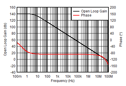
 Open-Loop Gain and Phase vs Frequency
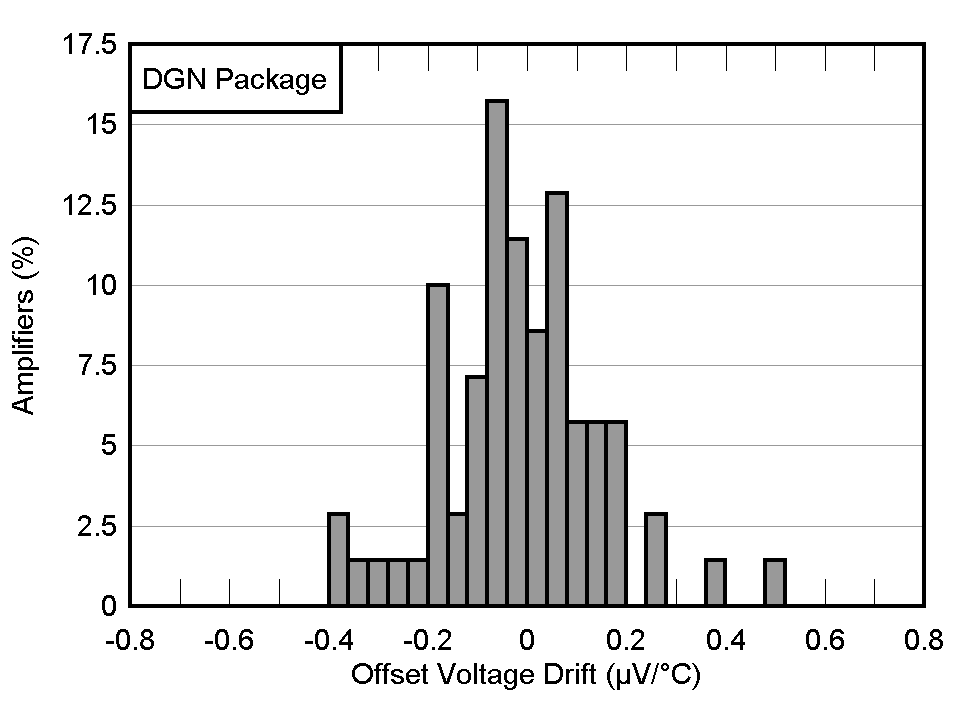
 Offset Voltage Drift